Location-specific NAND (ls NAND) memory technology and cells

a technology of location-specific nand and memory cells, which is applied in the direction of digital storage, instruments, semiconductor devices, etc., can solve the problems of complex and costly technology, cell technology never mainstream non-volatile cells, and difficult if not impossible complete removal of charge stored in nitrid

Inactive Publication Date: 2007-05-31
THOMAS MAMMEN
View PDF3 Cites 39 Cited by
  • Summary
  • Abstract
  • Description
  • Claims
  • Application Information

AI Technical Summary

Problems solved by technology

It has been seen that the complete removal of charge stored in the Nitride is difficult if not impossible by application of high voltages, even with adjustment of the trap location in the Nitride close to the silicon substrate.
Due to this reason of difficulty in erasing the cells the cells were never mainstream non-volatile cells used in NVM applications.
The technology hence is very complex and costly.
Since in a NAND structure a cell has multiple storage gates, each having its own storage element that are arranged in series across a source and drain, it is not possible to apply the necessary voltage to the junctions adjacent to each of the storage elements to cause CHE programming or B to B generation of holes very effectively.
Though programming can be with FN tunneling it is difficult to erase the cells with FN tunneling.
CHE allows two bit storage in mirror bit which will not be possible with FN tunneling programming.
B to B erase is not suitable for erasing a NAND structure, thus providing no suitable erase capability for a NAND structure with Location specific storage elements.
The high junction voltages also have the problem of increasing the channel lengths of the devices to eliminate punch through and leakage effects.
Junctions have to be made deep to withstand very high voltages without breakdown, this is counter to what is suitable for scaling.
Drain engineering is a complex process for these high voltage junctions.
It is made more complex by the need for location specific program and erase when hot electron programming and Band to Band tunneling erase are used.
The devices are slow to write.
The high current and high voltages translate to high power dissipation during program and erase.
Need for high voltage devices in the data path tend to limit access speed.
High process complexity and circuit complexity due to multiple voltage levels and polarity needs.
The necessity to ensure that the cells do not over erase, causing unselected cells to conduct during read, make the circuitry for program-erase complex.
The one major impediment to the development and implementation of the LS memory has been the difficulty in erasing the cells consistently.
The Band to Band Tunneling generation of holes for erase of the LS memory cell is a difficult process to optimize and it does not allow itself to be used in LS NAND structures.
In the case of LS memories the erase in the past has been the more difficult, and limiting operation.
Making sure that the traps exist closer to the interface consistently has been a difficult if not impossible requirement in manufacturing and this has been a problem with LS storage cells, especially Nitride based storage cells.
In addition having low thickness barrier to channel has the disadvantage of limited charge retention, resulting in low reliability of memory.
These issues of reliability and manufacturability has kept the prior art LS Nitride cells from becoming mainstream non-volatile storage cells.
Though the Mirror-bit cell provides a reasonable erase method, it by the complexity of drain design, make manufacturing and yielding of the technology difficult.
Since the program and erase use high voltages applied to junctions, this type of program using CHE generation and erase using B-to-B hole generation is not easily suited for NAND operation.
Typical NAND structures in silicon are used with FN tunneling for program and opposite direction FN tunneling for erase, which combination is not suitable for LS based cells as already explained.

Method used


Image

  • Location-specific NAND (ls NAND) memory technology and cells
  • Location-specific NAND (ls NAND) memory technology and cells
  • Location-specific NAND (ls NAND) memory technology and cells

Examples


Embodiment Construction

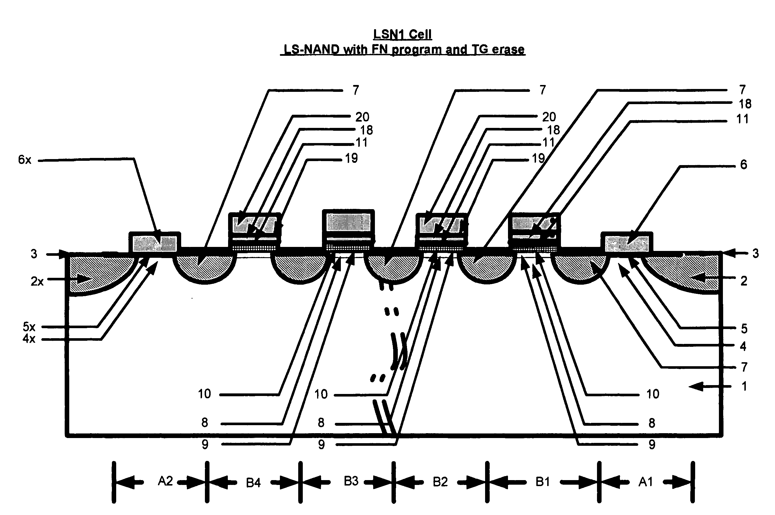
[0130] The current disclosure of LS based NAND cells are explained using two separate types of NAND cells. The difference between the two is in the programming method used. The cell shown in FIG. 5 uses FN Tunneling for programming the selected storage gates, while the cell shown in FIG. 6 uses Low-current Channel Hot Electron for programming the selected storage gates. In both cases the cells or arrays are erased using the TG to generate and supply the carriers, typically holes to neutralize the stored electron charge of the cell.

[0131] In the first instance, FIG. 5 is a NAND cell which is programmed by FN tunneling and erased by TG method. The NAND cell shown comprise of four storage gates or segments (B1 to B4) and two select gates (A1 and A2) that help isolate the cell if it is not a selected cell in the array. The four gates are shown as exaple and should not be construed as limiting the number of gates that can be implemented in the cell. The storage gate number can be increa...


PUM

PropertyMeasurementUnit
voltageaaaaaaaaaa
voltageaaaaaaaaaa
voltageaaaaaaaaaa

Abstract

The use of a Nitride layer or a silicon-nodule layer capable of location-specific (LS) charge storage, allow easy vertical scaling and implementation of NOR and NAND NVM array and technology. If the charge is stored in the traps in the Nitride storage layer, a Oxide Nitride Oxide is used as the storage element and if charge is stored in potential wells of discrete silicon-nodules, or Carbon Bucky-ball layers, an Oxide silicon-nodule Oxide storage element, or an Oxide Bucky-ball Oxide layer is used as the storage element. The problem of location-specific NAND memory is the inability to erase the cells with repeatable results. A novel erase method, Tunnel Gun (TG) method, that generate holes for consistent erase of LS storage elements and typical NAND Cells that erase by the disclosed method and programmed by either by Fouler-Nordheim (FN) tunneling or Low Current Hot Electron (LCHE) method are disclosed.

Description

FIELD OF INVENTION [0001] This invention relates to the structure and method of Programmable / Erasable Non-Volatile Memory cell technology for data storage applications. BACKGROUND [0002] Data storage in discrete locations in non conducting traps in Silicon Nitride layers or in barrier isolated potential wells in silicon nodule layers and carbon bucky ball layers, have been considered possibilities for non Volatile applications instead of the typical floating gate made of poly-silicon, for vertical scaling of the Non-Volatile Memory cells. These cells are called Location-Specific (LS) Charge storage cells as the charge is stored in discrete isolated traps or discrete potential wells in specific locations in the storage element and does not spread during operation. The problem has been mainly the erase of these cells, typically they require high voltages to be applied to the junctions and the wells to erase these types of cells as extracting charge from traps or potential wells comple...

Claims


Application Information

Patent Timeline
Patent Type & Authority Applications(United States)
IPC IPC(8): G11C16/04
CPCG11C16/0466G11C16/0483G11C16/12G11C16/16H01L27/115H01L27/11521H01L29/7881H10B69/00H10B41/30H10B41/35
Inventor THOMAS, MAMMEN
Owner THOMAS MAMMEN
Why Eureka
Try Eureka