Antenna and manufacturing method thereof, semiconductor device including antenna and manufacturing method thereof, and radio communication system

a manufacturing method and antenna technology, applied in the direction of resonant antennas, radiating elements, instruments, etc., can solve the problems of reducing resistance, difficult to increase the thickness of the antenna formed by screen printing, and difficult to improve the yield, so as to reduce the probability of the antenna being completely disconnected, increase the film thickness, and reduce the resistance materially

Active Publication Date: 2007-05-31
SEMICON ENERGY LAB CO LTD
View PDF13 Cites 37 Cited by
  • Summary
  • Abstract
  • Description
  • Claims
  • Application Information

AI Technical Summary

Benefits of technology

[0005] Thus, a conventional antenna has difficulty being reduced in resistance and improved in the yield. Therefore, a conventional semiconductor device for inputting / outputting data by radio communication with the antenna has difficulty having longer communication distance and higher reliability, and being reduced in cost.
[0027] The semiconductor integrated circuit can be provided so as to be electrically connected to the first pattern or the second pattern in the contact hole penetrating through the first substrate to reach the first pattern or the contact hole penetrating through the second substrate to reach the second pattern. Thus, the antenna can be prevented from being exposed to the outside as much as possible, and the antenna and the semiconductor integrated circuit can be electrically connected, which results in further enhanced reliability of the semiconductor device.

Problems solved by technology

It is difficult to increase a thickness of an antenna formed by screen printing, as well as reduce resistance thereof.
In addition, it is difficult to improve the yield.
Note that a method where the surface of an antenna is plated has more steps, which costs more.
In addition, the plating method has a limit to increase film thickness of an antenna.
In the case of employing a configuration where coiled antennas of the plurality of substrates are arranged so as to overlap with each other and electrically connected in series, it is difficult to reduce resistance of an antenna.
Further, if even one of a plurality of coiled antennas is partially disconnected, the plurality of antennas does not function normally.

Method used


Image

  • Antenna and manufacturing method thereof, semiconductor device including antenna and manufacturing method thereof, and radio communication system
  • Antenna and manufacturing method thereof, semiconductor device including antenna and manufacturing method thereof, and radio communication system
  • Antenna and manufacturing method thereof, semiconductor device including antenna and manufacturing method thereof, and radio communication system

Examples


embodiment mode 1

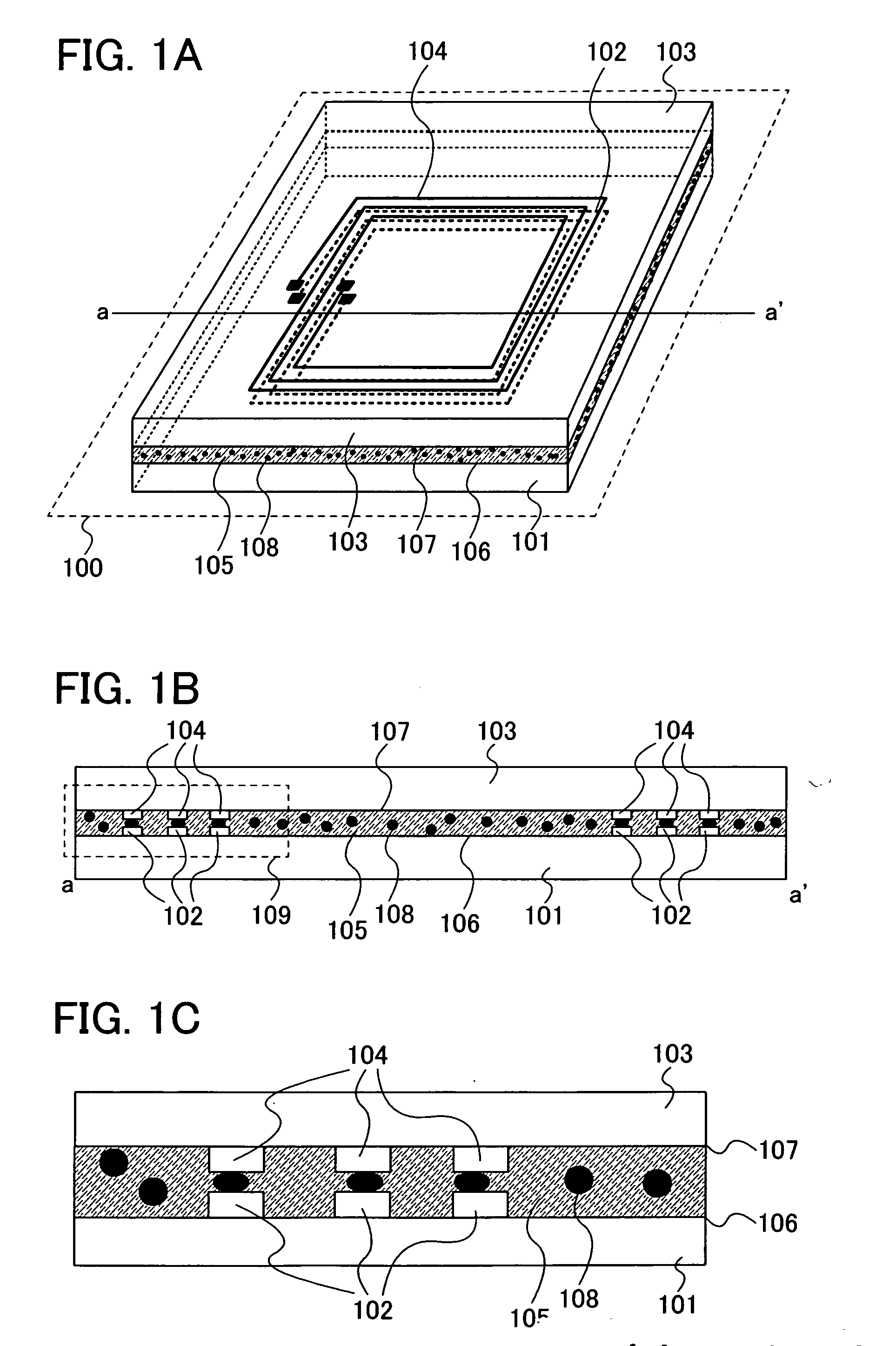
[0043] A structure of an antenna of the invention is described. FIGS. 1A to 1C each show a structure of the antenna. FIG. 1A shows a perspective view of an antenna. FIG. 1B shows a cross-sectional view taken along line A-A′ in FIG. 1A. FIG 1C shows an enlarged view of a region 109 in FIG. 1B. Note that common portions are denoted by the same reference numerals in FIGS. 1A to 1C. An antenna 100 includes a first substrate 101, a first pattern 102, a second substrate 103, a second pattern 104, and an anisotropic conductive material 105. The first substrate 101 has a first insulating surface 106. The first pattern 101 is formed of a conductive material, over the first insulating surface 106. The second substrate 103 is provided so as to face the surface of the first substrate 101, over which the first pattern 102 is formed, and has a second insulating surface 107. The second pattern 104 is formed of a conductive material, over the second insulating surface 107. The anisotropic conductiv...

embodiment mode 2

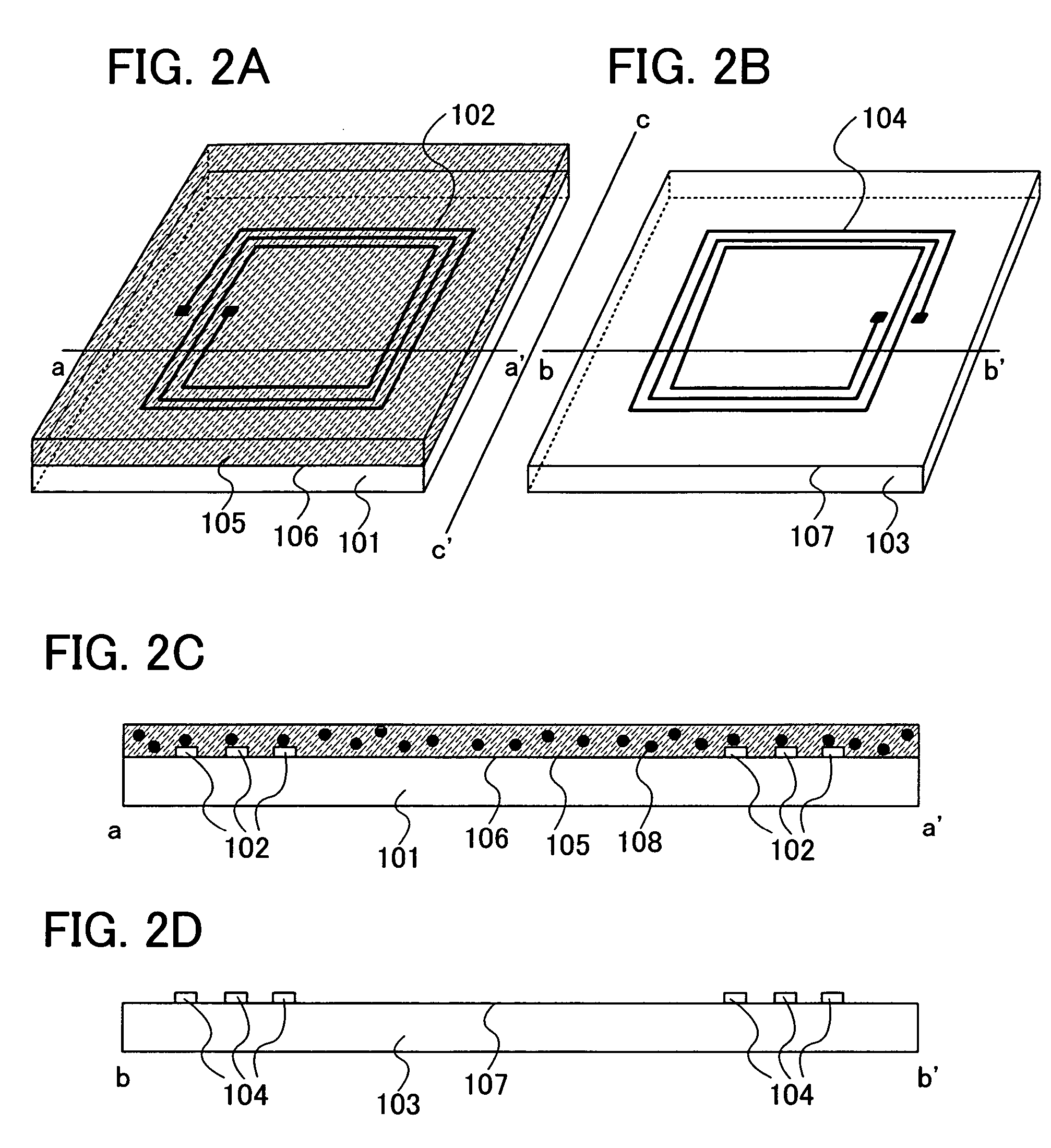
[0055] Description is made of a manufacturing method of an antenna of the invention with reference to FIGS. 2A to 2C. Note that common portions to those in FIGS. 1A to 1C are denoted by the same reference numerals, and description thereof is omitted.

[0056] As shown in FIG. 2A, the first pattern 102 is formed of a conductive material, over the first insulating surface 106 of the first substrate 101. The first pattern 102 can be formed by a droplet discharging method or a printing method. Note that a conductive film may be etched using photolithography or the like to form the first pattern 102. Subsequently, the anisotropic conductive material 105 is formed so as to cover all over the first pattern 102. In FIG. 2A, the conductive particles 108 in the anisotropic conductive material 105 are not shown. FIG. 2A shows an example where the anisotropic conductive material 105 is formed so as to cover all over the first insulating surface 106. Note that FIG. 2C shows a cross-sectional view ...

embodiment mode 3

[0065] Description is made of a structure of a semiconductor device of the invention with reference to FIGS. 3A to 3C. Note that common portions to those in FIGS. 1A to 2D are denoted by the same reference numerals, and description thereof is omitted.

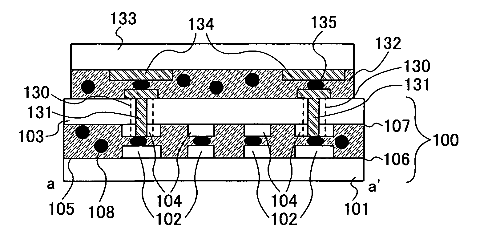
[0066]FIG. 3A shows a perspective view of a semiconductor device. FIG. 3B and 3C each show a cross-sectional view taken along line A-A′ in FIG. 3A. Note that common portions to those in FIGS. 1A to 1C are denoted by the same reference numerals. A semiconductor device 300 includes the antenna 100 and a semiconductor integrated circuit 133 electrically connected to the antenna 100. The semiconductor device 300 transmits / receives a radio signal by the antenna 100, and inputs / outputs data.

[0067] As shown in FIG. 3B, a pair of contact holes 130 penetrating through the second substrate 103 to reach the second pattern 104 are provided. In a structure in FIG. 3B, the contact holes 130 do not penetrate through the second pattern 104. An electr...


PUM


Abstract

An antenna includes a first substrate, a first pattern, a second substrate, a second pattern, and an anisotropic conductive material. The first substrate has an insulating surface. The first pattern is formed over the insulating surface of the first substrate, and made of a conductive material. The second substrate is provided so as to face the surface over which the first pattern of the first substrate is formed and has an insulating surface. The second pattern is formed over the insulating surface facing the first substrate of the second substrate, and made of a conductive material. The anisotropic conductive material electrically connects the first pattern and the second pattern. The whole region of the first pattern overlaps with the second pattern with the anisotropic conductive material interposed therebetween.

Description

TECHNICAL FIELD [0001] The present invention relates to an antenna and a manufacturing method thereof. The invention also relates to a semiconductor device which includes an antenna and a semiconductor integrated circuit electrically connected to the antenna, and inputs / outputs data by radio communication through the antenna. In addition, the invention relates to a radio communication system including the semiconductor device and a reader / writer which inputs / outputs data by radio communication. BACKGROUND ART [0002] Identification technology where an ID (identification number) is assigned to an individual object so as to clarify the history thereof, which is utilized for production, management, and the like has been attracting attention. Above all, RFID (Radio Frequency Identification) technology using a semiconductor device for inputting / outputting data through radio communication, such as a radio tag (also referred to as an IC tag, an IC chip, an RF (Radio Frequency) tag, an RFID,...

Claims


Application Information

Patent Timeline
Patent Type & Authority Applications(United States)
IPC IPC(8): H01L21/8234H01L21/44H01L23/52
CPCH01L23/49822H01L23/49827H01L2924/0002H01L23/49855H01L23/49883H01L23/528H01L23/564H01L23/66H01L25/16H01L27/1214H01L27/1266H01L27/13H01L2223/6677H01L2924/12044H01Q1/38H01Q9/27H05K3/323H01L2924/00G06K19/077H01L21/18H01Q1/24
Inventor AOKI, TOMOYUKI
Owner SEMICON ENERGY LAB CO LTD
Why Eureka
Try Eureka