

Substrate and substrate module
- Summary
- Abstract
- Description
- Claims
- Application Information
AI Technical Summary
Benefits of technology
Problems solved by technology
Method used
Image

Examples
Embodiment Construction
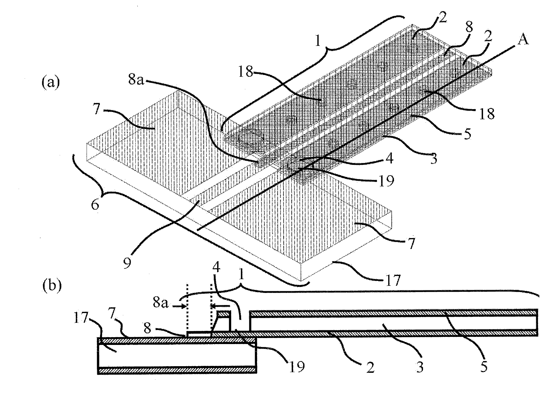
[0039] The present invention is directed to a connection substrate for connecting a substrate on which circuits such as a drive circuit for driving a laser device, and an amplifier for amplifying signals from a photo acceptance device are mounted, to a laser device and / or a photo acceptance device; and directed to a substrate module using the above-described substrate.
[0040] Hereinafter, an embodiment according to the present invention will be described with reference to accompanying drawings. Throughout the drawings, the same or functionally equivalent parts are designated with the same reference numerals.
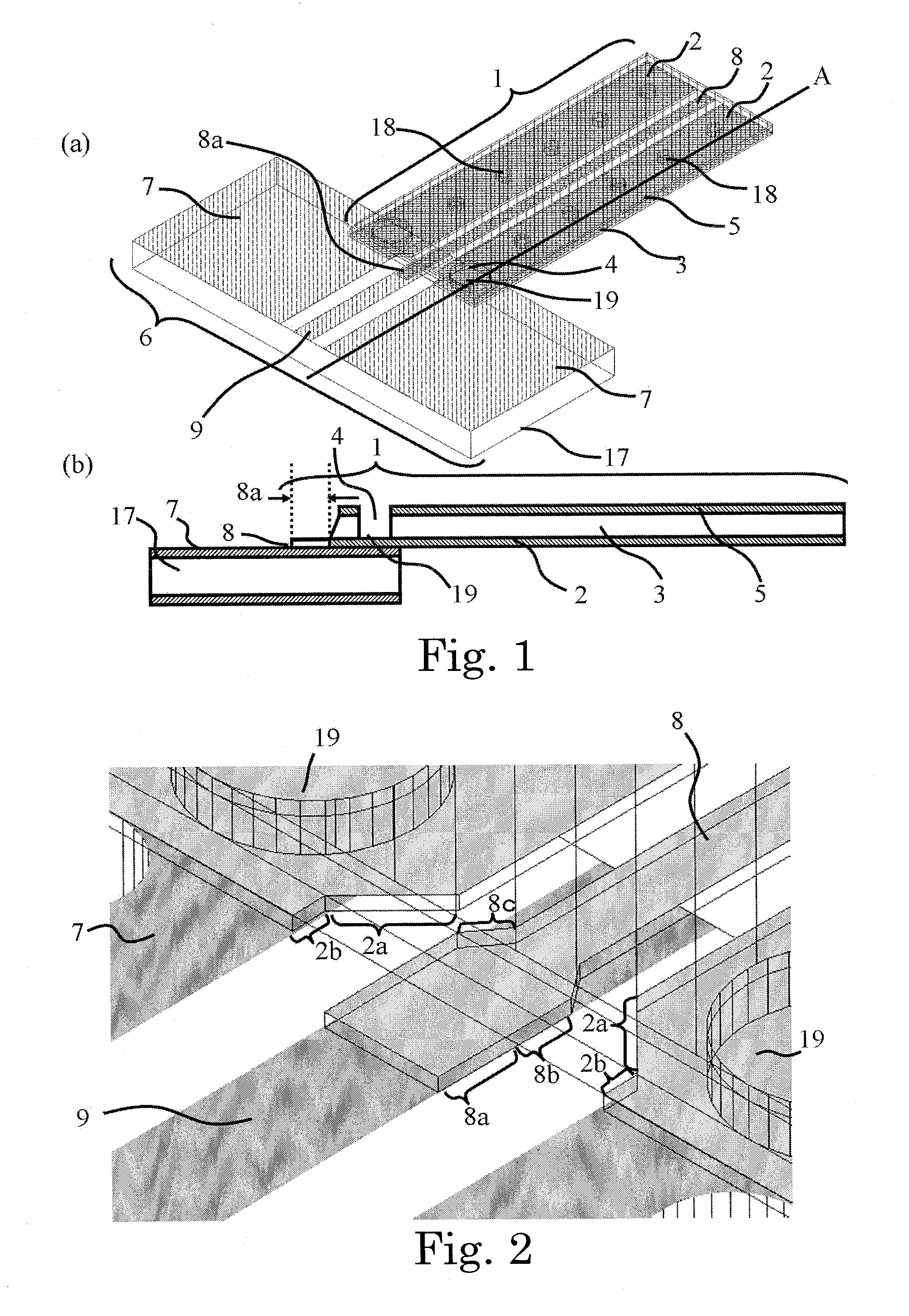
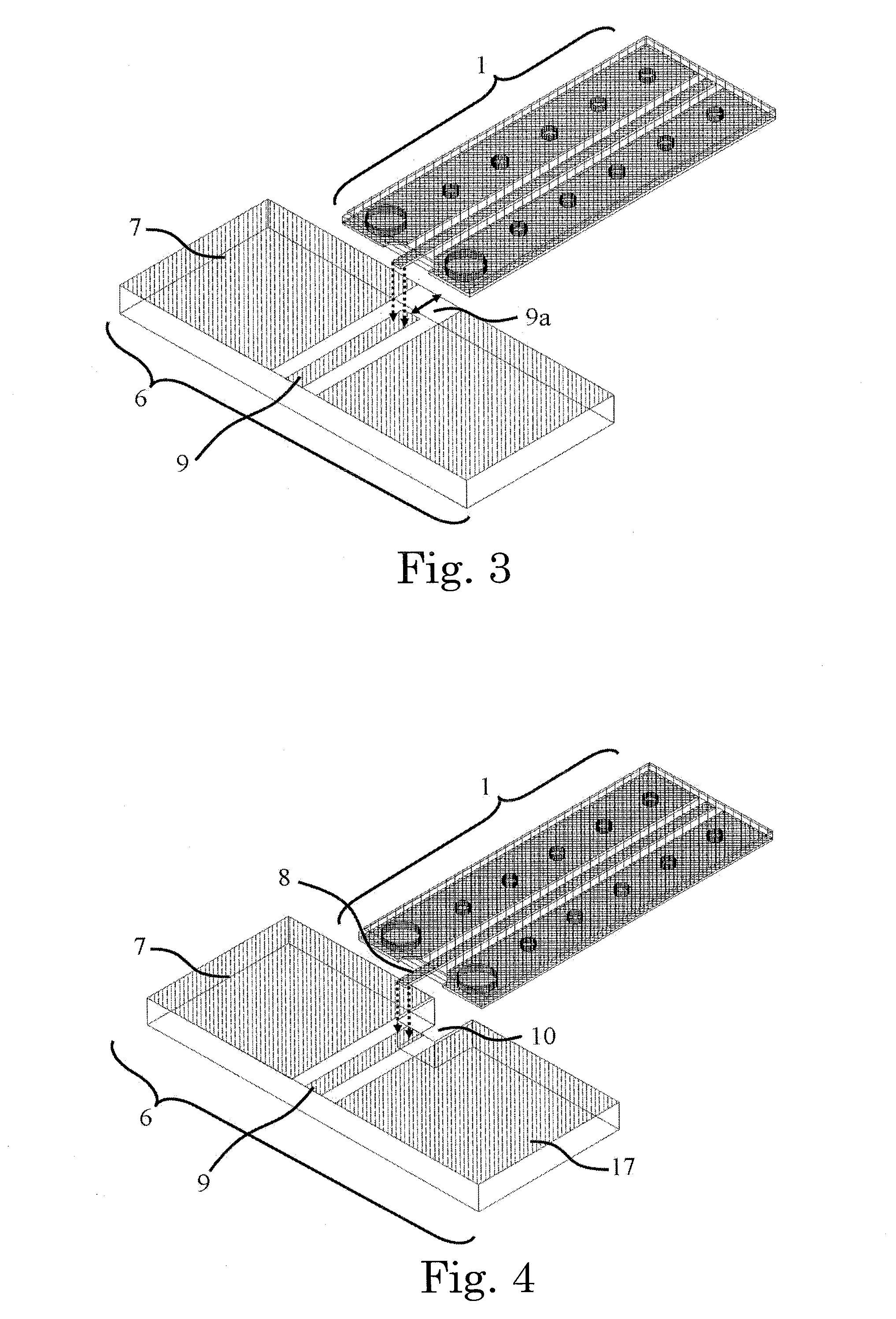
[0041]FIGS. 1A and 1B are each a representation of the embodiment according to present invention. FIG. 1A is a perspective view of a substrate for connection and a substrate on which electric circuitry is mounted. FIG. 1B is a sectional view of these substrates cut taken away along a line A in FIG. 1A.
[0042] The substrate 1 for connecting a light receiving / emitting element betw...
PUM
 Abstract
Description
Claims
Application Information