Method for measuring physical quantity of measurement object in substrate processing apparatus and storage medium storing program for implementing the method

a technology of substrate processing and measurement objects, applied in the direction of heat measurement, optical radiation measurement, instruments, etc., can solve the problems of inability to achieve an accurate measurement of a predetermined physical quantity, inability to measure the temperature of substrates with accuracy, and change in optical fiber length

Active Publication Date: 2007-06-07
TOKYO ELECTRON LTD
View PDF23 Cites 27 Cited by
  • Summary
  • Abstract
  • Description
  • Claims
  • Application Information

AI Technical Summary

Benefits of technology

[0008] An object of the invention is to provide a method for measuring a physical quantity of a measurement object in a substrate processing apparatus that is

Problems solved by technology

However, the substrate is mainly made of silicon whose infrared emission characteristic changes at a temperature of about 600 degrees Celsius, and therefore, the substrate temperature cannot be measured with accuracy, especially at low temperatures, by the radiation thermometer.
Since the optical path length is affected by a change in optical fiber length, it is difficult to accurately measure the optical path length of th

Method used


Image

  • Method for measuring physical quantity of measurement object in substrate processing apparatus and storage medium storing program for implementing the method
  • Method for measuring physical quantity of measurement object in substrate processing apparatus and storage medium storing program for implementing the method
  • Method for measuring physical quantity of measurement object in substrate processing apparatus and storage medium storing program for implementing the method

Examples


first embodiment

[0046] First, an explanation will be given of a substrate processing apparatus to which is applied a method for measuring a physical quantity of a measurement object according to the present invention.

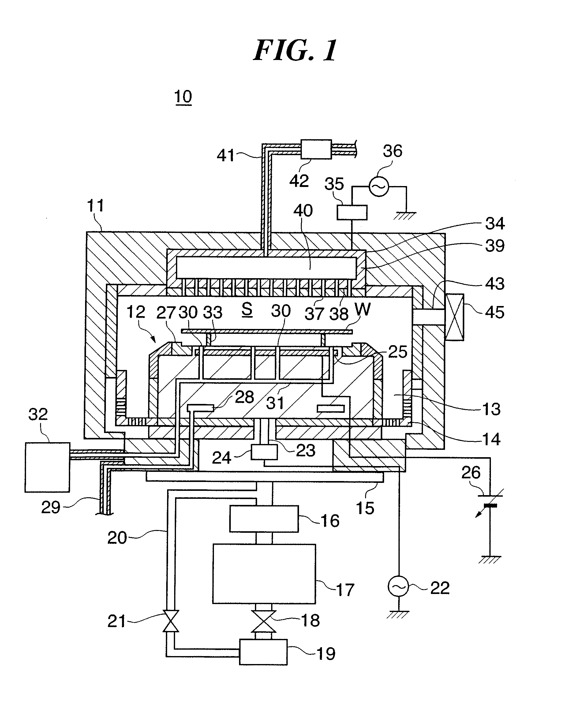
[0047]FIG. 1 is a section view showing a schematic construction of the substrate processing apparatus. A plasma processing apparatus as the substrate processing apparatus is designed that a semiconductor wafer W as a substrate (hereinafter simply referred to as the “wafer W”) is subjected to plasma processing such as RIE (Reactive Ion Etching) and ashing.

[0048] Referring to FIG. 1, the plasma processing apparatus 10 includes a cylindrical chamber 11 made of aluminum and having a wall whose inner surface is coated with anodized aluminum. In the chamber 11, a cylindrical mounting table 12 is disposed, which serves as a stage for mounting thereon the wafer W having a diameter of, e.g., 300 mm.

[0049] In the plasma processing apparatus 10, a gas exhaust path 13, serving as a channel for d...

second embodiment

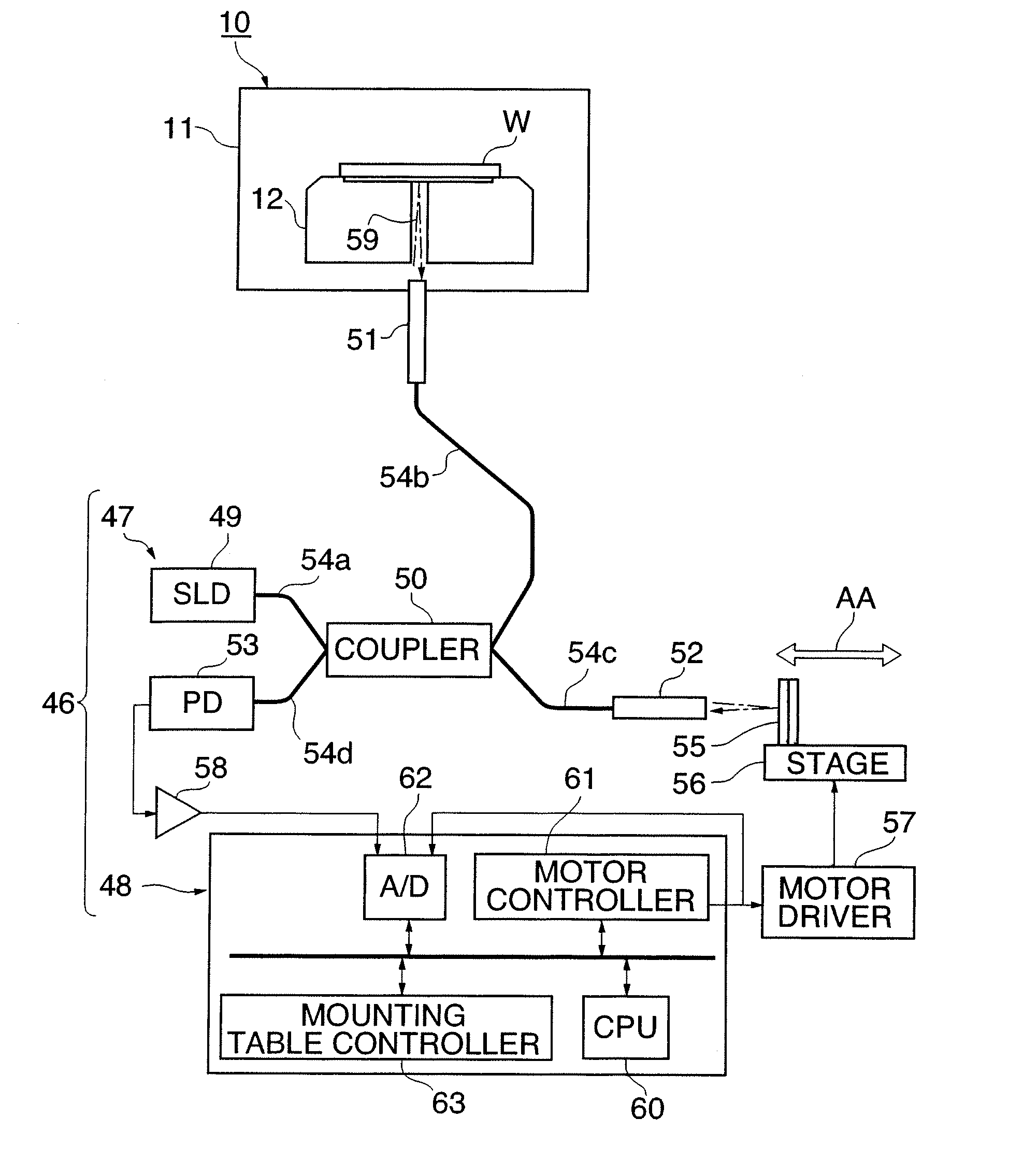
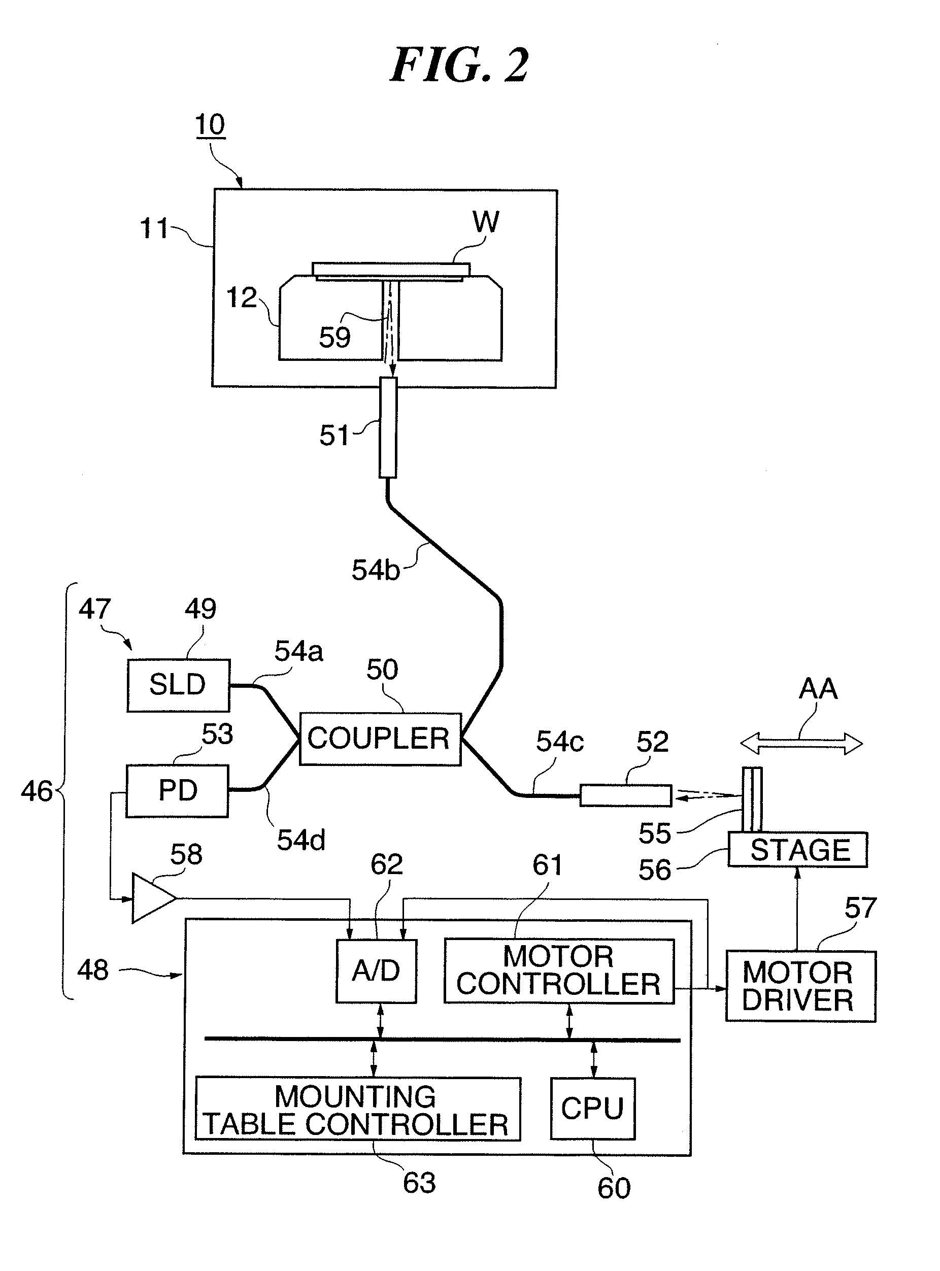
[0094] Next, an explanation will be given of a method for measuring a physical quantity of a measurement object in a substrate processing apparatus according to the present invention.

[0095] As described above, in many cases, the tendency of change in the ambient temperature around the optical fiber 54b is stable. However, the tendency of the temperature change can sometimes be unstable for any accidental factors. For instance, in some cases, the increasing speed of the ambient temperature around the optical fiber 54b can vary, resulting in a change in the speed of increasing the temperature of the optical fiber 54b. Thus, in the method of physical quantity of the measurement object in the substrate processing apparatus of the present embodiment, the interference position differences DD′, DD″ in the forward and backward strokes are individually corrected.

[0096] The present embodiment is the same in construction and function as the aforementioned first embodiment but differs therefro...

third embodiment

[0108] Next, an explanation will be given of a method for measuring a physical quantity of a measurement object of a substrate processing apparatus according to the present invention.

[0109] The present embodiment is basically the same in construction and function as the first embodiment, and only differs therefrom in that the way of determining the optical length path is changed based on the rate of change in ambient temperature in the forward stroke and that in the backward stroke. Thus, the duplicate explanation on the common construction and function will be omitted, and an explanation will be given of only on different construction and function.

[0110]FIG. 10 is a flowchart showing a wafer temperature measuring process in the present embodiment.

[0111] Referring to FIG. 10, the CPU 60 causes the reference mirror 55 to move in the direction away from the collimator fiber 52, measures interference positions PA and PB in the forward stoke at timings TA and TB, respectively (step S1...


PUM


Abstract

A method capable of accurately measuring a physical quantity of a measurement object in a substrate processing apparatus. In a temperature measurement apparatus for implementing the method, two interference positions are measured at different timings when a reference mirror is caused to move in the direction away from a collimator fiber, and a difference between the two interference positions is calculated. When the reference mirror remote from the collimator fiber is caused to move toward the collimator fiber, two interference positions are measured at different timings, and a difference between the two interference positions is calculated. An average value of the interference position differences is calculated, an optical path length difference is determined from the average value, and a wafer temperature is calculated from the optical path length difference.

Description

BACKGROUND OF THE INVENTION [0001] 1. Field of the Invention [0002] The present invention relates to a method for measuring a physical quantity of a measurement object in a substrate processing apparatus, and more particularly, to a physical quantity measuring method utilizing, for measurement, interference of irradiation light and reflected light, and a storage medium storing a program for implementing the measuring method. [0003] 2. Description of the Related Art [0004] A substrate processing apparatus for plasma-processing a substrate such as a semiconductor device wafer has strongly been demanded to be capable of contactlessly measuring the temperature of a wafer housed in a processing chamber of the substrate processing apparatus. As a contactless thermometer, a radiation thermometer has been known that measures the temperature of a measurement object based on infrared radiation emitted from the measurement object. However, the substrate is mainly made of silicon whose infrared...

Claims


Application Information

Patent Timeline
IPC IPC(8): G01B11/02G01B9/02
CPCG01J5/0003G01J2005/583G01K5/52G01K11/00G01K11/3206G01B9/02019G01B9/02028G01B9/0209G01B9/02023G01B9/02083
Inventor KOSHIMIZU, CHISHIOSUZUKI, TOMOHIRO
Owner TOKYO ELECTRON LTD
Why Eureka
Try Eureka