Nonvolatile semiconductor memory

a semiconductor memory and non-volatile technology, applied in static storage, digital storage, instruments, etc., can solve the problems of difficulty in reducing the layout area of the array, increase the area occupied by the memory cell array, and increase the layout area of the memory cell array. , to achieve the effect of quick readout of data, increased layout area of the memory cell array, and fast readout of data

Inactive Publication Date: 2007-06-07
RENESAS ELECTRONICS CORP
View PDF3 Cites 14 Cited by
  • Summary
  • Abstract
  • Description
  • Claims
  • Application Information

AI Technical Summary

Benefits of technology

[0026] With the nonvolatile semiconductor memory according to the invention, the dummy cells are laid out so as to be lined up with respective memory cell columns, and the respective memory cell columns and the dummy cells are coupled to the respective bit lines. At the time of selection of the dummy cell, the source line in a column adjacent thereto is coupled to the bit line corresponding thereto. Accordingly, when the source line in the adjacent column is in a select state, a current flows to the bit line coupled to the dummy cell via the first and second switching transistors, thereby causing a potential change to occur to the bit line corresponding to the source line. Meanwhile, with the respective memory cells coupled to the source line in the select column, a current flows selectively via the cell select transistor, and the data storage. In consequence, there occurs a difference in potential-change speed between the...

Problems solved by technology

Accordingly, with the mask ROM of the high-speed specification, it is possible to implement quick access substantially equivalent to that for an SRAM (Static Random Access Memory), however, since two memory cells are used for storing 1-bit data, there arises a problem of an increase in area occupied by a memory cell array.
Accordingly, there arises the need for changing the position of the bit line within the array, thereby causing a problem in that a wiring layout becomes complex.
Furthermore, the bit line with the memory cells connected thereto is utilized as the reference bit line, however, as the dummy cells connected to the reference bit line is disposed outside the memory cell array, there arises a problem of difficulty in reducing an array layout area.
Further, in order to make use...

Method used


Image

  • Nonvolatile semiconductor memory
  • Nonvolatile semiconductor memory
  • Nonvolatile semiconductor memory

Examples


embodiment 1

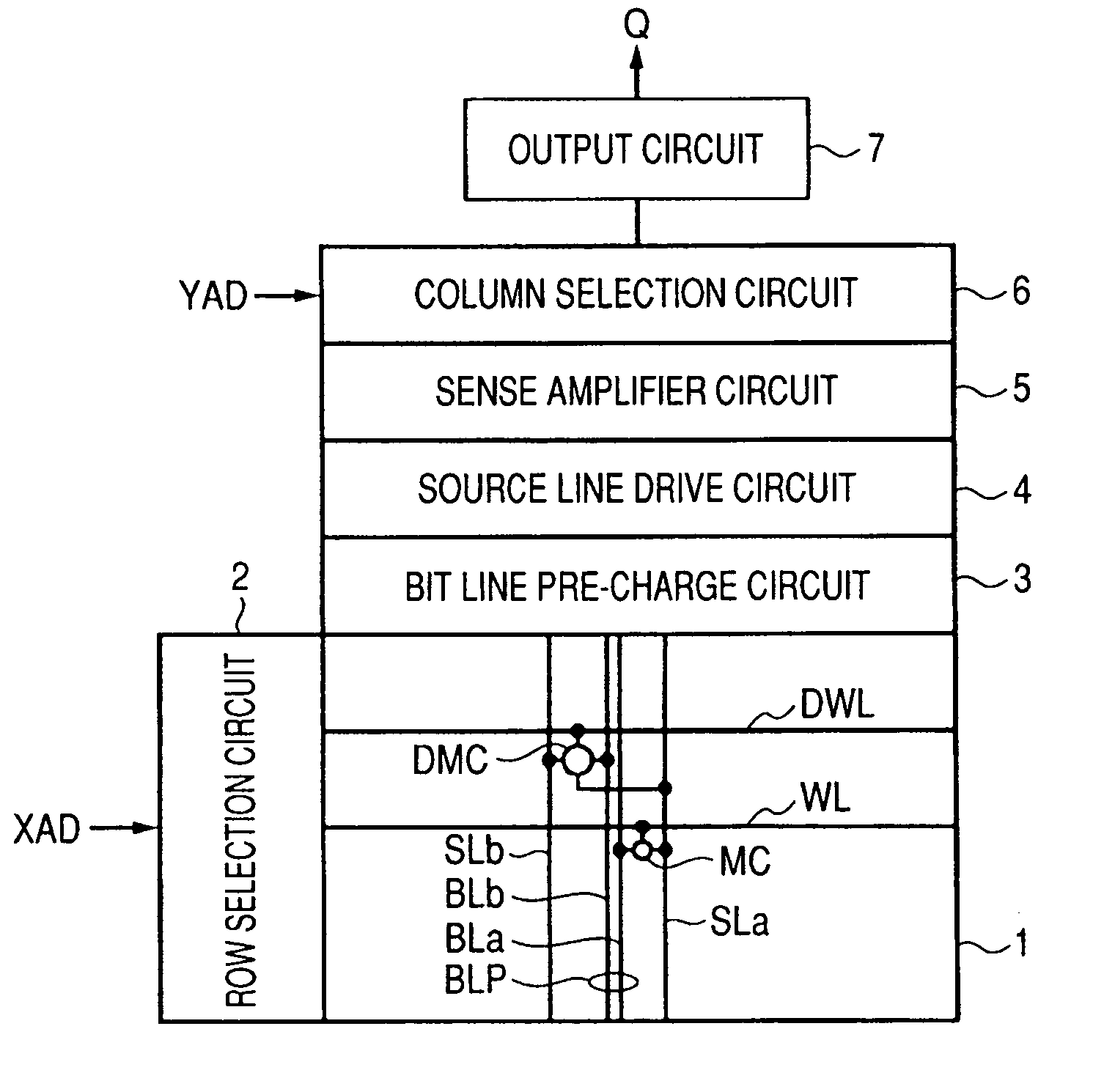
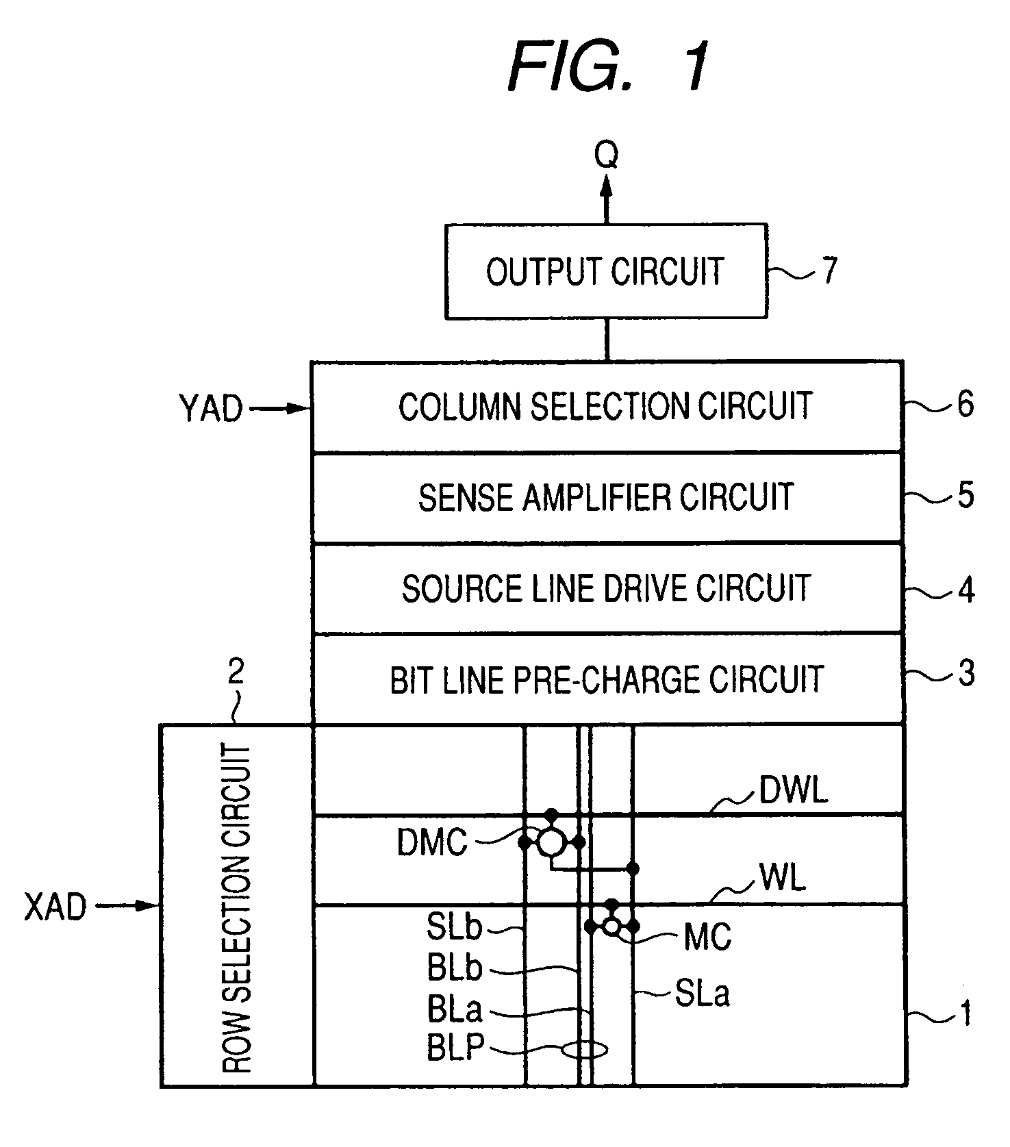
[0035]FIG. 1 is a view broadly showing a whole configuration of Embodiment 1 of a nonvolatile semiconductor memory according to the invention. In FIG. 1, the nonvolatile semiconductor memory includes a memory cell array 1 where nonvolatile memory cells MC are arranged in a matrix fashion. With the nonvolatile memory cell MC, stored data thereof is set by mask wiring.

[0036] In the memory cell array 1, word lines WL are laid out so as to correspond to respective rows of the memory cells MC, and further, bit lines BL are laid out so as to correspond to respective columns of the memory cells MC. The bit lines are laid out so as to form a pair, respectively, and in FIG. 1, there is shown a bit line pair BLP formed by the bit lines BLa, and BLb, as a typical bit line pair.

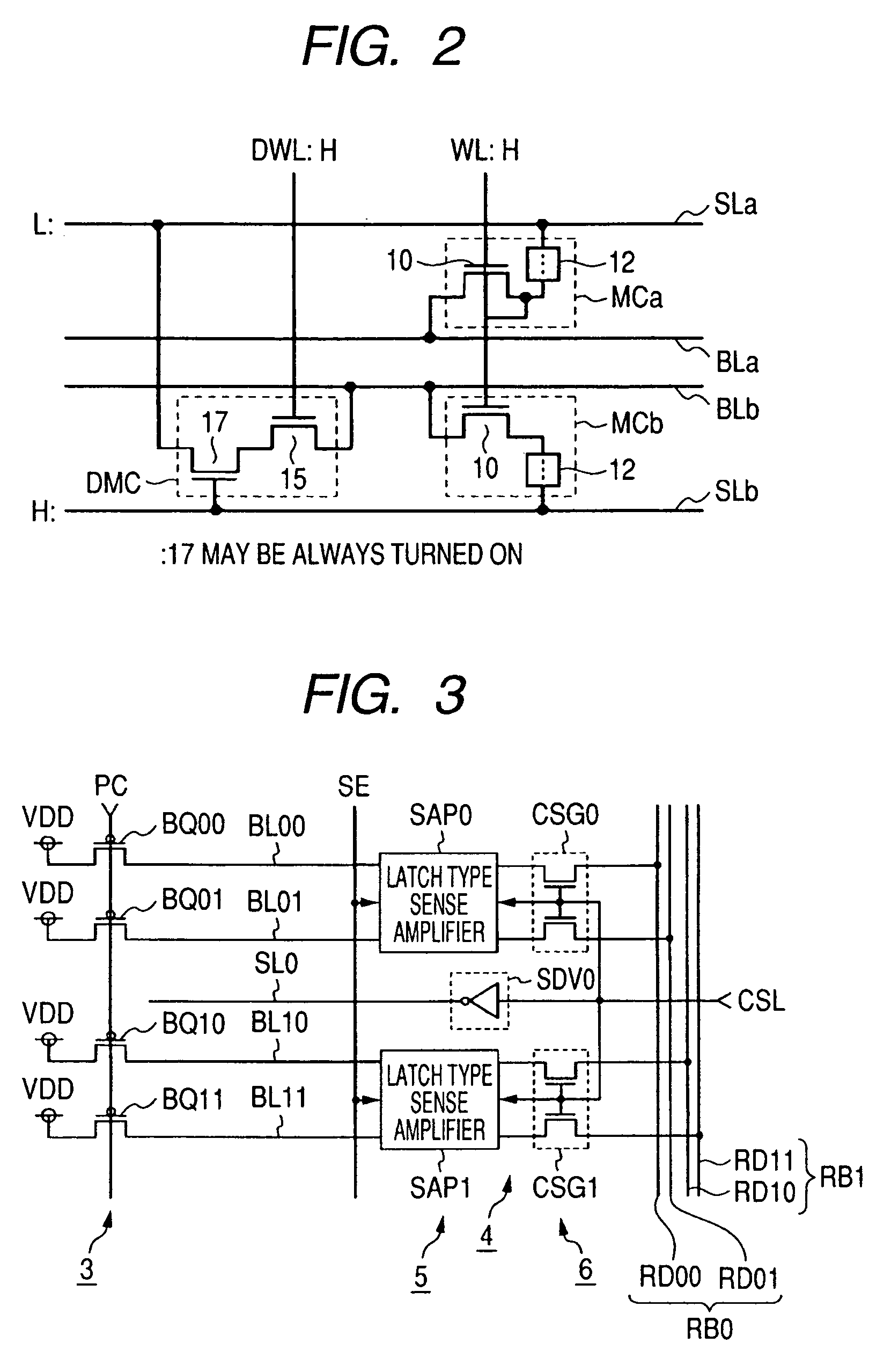
[0037] Further, in the memory cell array 1, there are provided dummy cells DMC disposed so as to be lined up in at least one row, and dummy word lines DWL coupled to the dummy cells DMC, disposed so as to be lined up i...


PUM


Abstract

There is provided a high-density mask ROM operable at a high speed. With the mask ROM, respective source lines are disposed so as to be shared by memory cells in respective columns adjacent to each other, and bit lines are disposed so as to correspond to the respective columns of the memory cells. Further, the dummy cells are disposed for the respective columns of the memory cells. The dummy cells are each made up of a series-circuit including a first switching transistor that is turned into the conducting state in response to a signal potential on a dummy word line (DWL), and a second switching transistor 17 for coupling an adjacent source line to the bit line corresponding thereto in response to a potential of the source line in a column corresponding thereto. The memory cells each are made up of one unit of a transistor and a data storage formed by mask wiring. At the time of reading data, a potential of the source line in a select column is caused to undergo a change, whereupon there occurs a potential difference between a pair made up of the bit line as selected to which the memory cells as selected are coupled, and a reference bit line with the dummy cells coupled thereto, so that it is possible to execute readout of data by detecting the potential difference.

Description

CROSS-REFERENCE TO RELATED APPLICATION [0001] The present application claims priority from Japanese patent application No. 2005-352384 filed on Dec. 6, 2005, the content of which is hereby incorporated by reference into this application. BACKGROUND OF THE INVENTION [0002] The invention relates to a nonvolatile semiconductor memory, and in particular, is concerned with a configuration of a mask ROM (Read Only Memory) wherein stored data is programmable by mask wiring. [0003] With the mask ROM, data is fixedly stored by selectively forming metal interconnections in a storage with the use of a mask for a wiring pattern during a manufacturing process. The mask ROM includes a NAND type mask ROM, or a NOR type mask ROM, depending on a configuration of interconnection among memory cells. With the NAND type mask ROM, a plurality of memory cells are connected in series to each other between a bit line and a source line. Further, as is so often the case, data is stored by adjusting the thresh...

Claims


Application Information

Patent Timeline
IPC IPC(8): G11C7/02
CPCG11C7/14G11C17/12
Inventor OKAMOTO, KAZUYOSHIYANAGISAWA, KAZUMASA
Owner RENESAS ELECTRONICS CORP
Why Eureka
Try Eureka