Process for fabricating a micro-electro-mechanical system with movable components

Inactive Publication Date: 2007-06-07
MATSUSHITA ELECTRIC WORKS LTD
View PDF0 Cites 22 Cited by
  • Summary
  • Abstract
  • Description
  • Claims
  • Application Information

AI Technical Summary

Benefits of technology

[0003] In view of the above insufficiency, the present invention has been accomplished to provide a unique process for fabricating a micro-electro-mechanical system (MEMS) composed of fixed components fixedly supported on a base and movable components movably supported on the base. The process utilizes an upper semiconductor substrate and a lower substrate which defines the base. A top layer in the upper substrate is selectively etched to form therein a plurality of posts which project commonly from a bottom layer of the upper substrate. The posts include the fixed components to be fixed to the lower substrate and the movable components which are resiliently supported only to one or more of the fixed components to be movable relative to the fixed components and the lower substrate. The lower substrate is also etched in its top surface to form therein at leas

Problems solved by technology

That is, as the gap is required to be greater for assuring the movable components free from being interfered with the base, the height of the fixed components are mad

Method used


Image

  • Process for fabricating a micro-electro-mechanical system with movable components
  • Process for fabricating a micro-electro-mechanical system with movable components
  • Process for fabricating a micro-electro-mechanical system with movable components

Examples


second embodiment

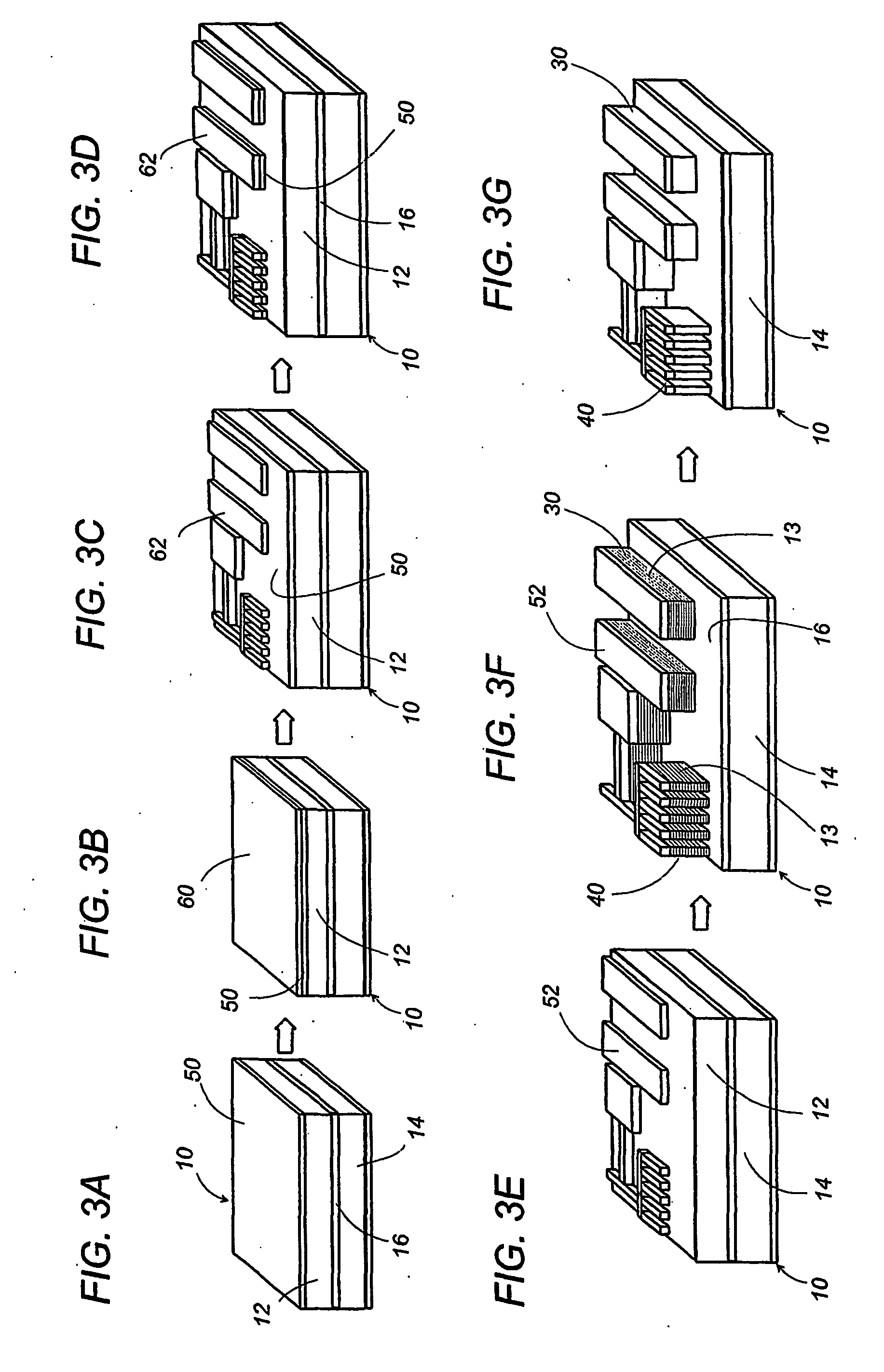
[0039]FIGS. 10 and 11 illustrate a process for fabricating the like a micro-electro-mechanical system (MEMS) in accordance with the second preferred embodiment which is similar to the above embodiment except for the use of the upper semiconductor substrate 10A made of a bare silicon monocrystal. The upper substrate 10A is firstly coated on its top with an oxide layer 50A formed by the thermal oxidation or the CVD process, and is masked With a resist pattern 62A, as shown in FIG. 10A. Then, the oxide layer 50 is etched to leave a mask 52A on top of the upper substrate 10A (FIG. 10B), after which the resist pattern 62A is removed off (FIG. 10C). Then, the upper substrate 10A is treated with the deep reactive ion etching (DRIE) to form the fixed components 30A and the movable components 40A commonly projecting on the bottom layer 14A of the upper substrate 10A, as shown in FIG. 10D. Next, the exposed faces of the components 30A and 40A are thermally oxidized in order to eliminate serra...

third embodiment

[0041]FIG. 12 illustrates a process for fabricating the like a micro-electro-mechanical system (MEMS) in accordance with the third preferred embodiment which is similar to the above embodiment except that it is contemplated to make the movable components 40A shorter in its height than the fixed components 30A. The movable components 40A may be required to be given a height shorter than the fixed components 30A for reason of leaving a large gap on the lower substrate 20A and / or adjusting the mechanical characteristics. In order to differentiate the height of the fixed and movable components, the present embodiment utilizes a composite mask composed of a first mask 52 and a second mask 54 which is etched at a higher rate than the first mask 52 but at a lower rate than the upper substrate 10A, i.e., silicon, when subjected to the same etching treatment. FIG. 12A shows the first mask 52 which is formed by selectively removing or etching away portions of the oxide layer formed on top of ...

fourth embodiment

[0042]FIG. 13 illustrates a useful scheme of etching away the bottom layer 14A of the upper substrate 10A in accordance with a fourth embodiment of the present invention. The present embodiment is particularly useful in case where the components are designed to be spaced laterally by largely varying widths, and where the upper substrate 10A is devoid of the buried oxide layer. In such case, cavities 15 of greatly different widths are to be left between the adjacent ones of the posts or the components 30A and 40A after the top layer 12A of the upper substrate 10A is etched away. It is true that, during the etching of the top layer, the growing cavities of greater widths are likely to be etched to a greater depth, which causes the finished cavities to have different depths, failing to align the bottoms of the cavities in the same level. Irrespective of the misaligned bottoms of the cavities, the present embodiment gives an easy etching control for releasing the components 30A and 40A ...


PUM

PropertyMeasurementUnit
Currentaaaaaaaaaa
Dielectric polarization enthalpyaaaaaaaaaa
Heightaaaaaaaaaa

Abstract

A process for fabricating a micro-electro-mechanical system (MEMS) composed of fixed components fixedly supported on a lower substrate and movable components movably supported on the lower substrate. The process utilizes an upper substrate separate from the lower substrate. The upper substrate is selectively etched in its top layer to form therein a plurality of posts which project commonly from a bottom layer of the upper substrate. The posts include the fixed components to be fixed to the lower substrate and the movable components which are resiliently supported only to one or more of the fixed components to be movable relative to the fixed components. The lower substrate is formed in its top surface with at least one recess. The upper substrate is then bonded to the top of the lower substrate upside down in such a manner as to place the fixed components directly on the lower substrate and to place the movable components upwardly of the recess. Finally, the bottom layer of the upper substrate is removed to release the movable components from the bottom layer for floating the movable components above the recess and allowing them to move relative to the lower substrate, while keeping the fixed components fixed to the top of the lower substrate.

Description

TECHNICAL FIELD [0001] The present invention relates to a process for fabricating a micro-electro-mechanical system (MEMS) composed of fixed components fixedly supported on a base and movable components movably supported on the base. BACKGROUND ART [0002] Japanese Patent Publication No. 03-230779 discloses a movable micromechanical system fabricated through micro-fabrication technology. The system includes fixed components and movable components both of which are formed from a common silicon substrate and are supported on a base made of a glass or semiconductor material. The common silicon substrate is etched to a limited depth or within a surface layer to form a plurality of posts which project commonly from a remainder layer of the silicon substrate. The posts include the fixed components and the movable components which are resiliently supported to one or more of the fixed components to be movable relative thereto. The silicon substrate is then bonded to the base with the fixed c...

Claims


Application Information

Patent Timeline
IPC IPC(8): H01L21/30B81B3/00B81C1/00B81C3/00G02B6/35G02B26/08H02N1/00
CPCB81B3/0086B81B2201/033B81B2201/045B81C1/00484B81C2201/0109B81C2201/019G02B6/3516G02B6/3518G02B6/3546G02B6/355G02B6/357G02B6/3584G02B26/0816H02N1/008B81B3/00G02B6/35B81C1/00B81C3/00
Inventor OKA, NAOMASAHARADA, HIROSHIOGIHARA, JUNFUKSHIMA, HIROSHINOGE, HIROSHISUZUKI, YUJIKAWANO, KIYOHIKOYOSHIHARA, TAKAAKISUZUMURA, MASAHIKO
Owner MATSUSHITA ELECTRIC WORKS LTD
Why Eureka
Try Eureka