Plasma process device and plasma process method

a plasma process and process technology, applied in the direction of plasma technique, coating, electric discharge lamps, etc., can solve the problems of lowering process uniformity, process with a sufficiently high uniformity may not be executed, difficult to optimize gas, etc., and achieve high uniformity

Inactive Publication Date: 2007-06-14
TOKYO ELECTRON LTD
View PDF5 Cites 17 Cited by
  • Summary
  • Abstract
  • Description
  • Claims
  • Application Information

AI Technical Summary

Benefits of technology

[0016] It is therefore an object of the invention to provide a plasma process system and a plasma process method which can perform a process with high uniformity on a subject to be processed.

Problems solved by technology

This makes the gas supply at the center portion and end portion of the to-be-processed subject W uneven, thus lowering the process uniformity.
Therefore, a process with a sufficiently high uniformity may not be executed.
It is therefore difficult to optimize the gas blowoff diameter and the upper electrode diameter by independently varying them to thereby improve the process uniformity.

Method used


Image

  • Plasma process device and plasma process method
  • Plasma process device and plasma process method
  • Plasma process device and plasma process method

Examples


first embodiment

[0068] A process system according to the first embodiment of the invention will now be described below with reference to the accompanying drawings. In the following embodiment to be illustrated below, a parallel plate plasma process system which forms a silicon fluoride oxide (SiOF) film on a semiconductor wafer (hereinafter “wafer W”) by CVD (Chemical Vapor Deposition) will be described as an example.

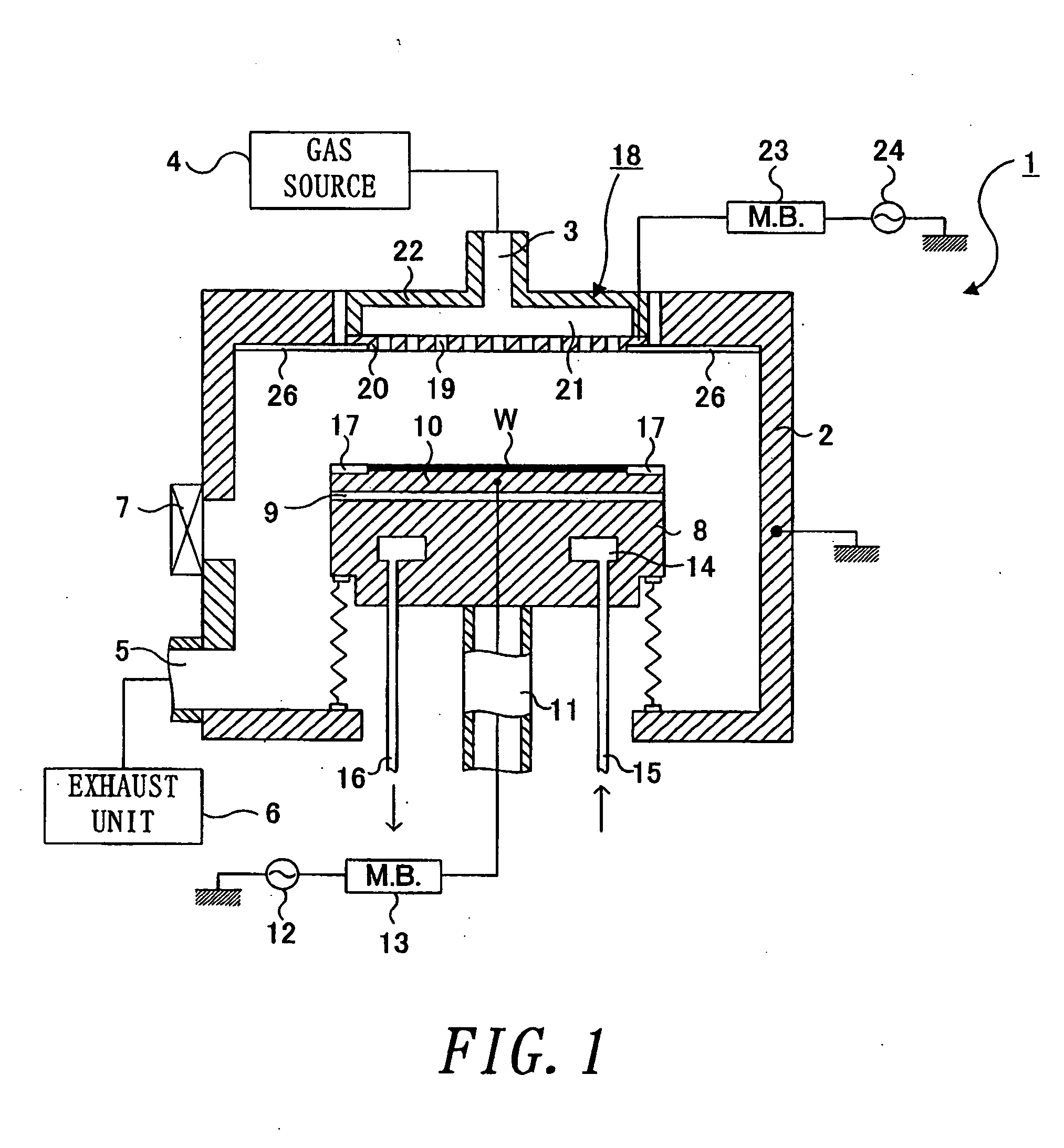
[0069]FIG. 1 illustrates the structure of a plasma process system 1 according to the first embodiment.

[0070] The plasma process system 1 has a cylindrical chamber 2 made of, for example, aluminum whose surface has been subjected to an alumite process (anodic oxidation). The chamber 2 is grounded to a common potential.

[0071] A gas supply tube 3 is provided in the upper portion of the chamber 2. The gas supply tube 3 is connected to a which supplies a process gas having a mixture of SiF4, SiH4, O2, Ar, etc. The process gas is adjusted to a predetermined flow rate by a mass flow contro...

example 1

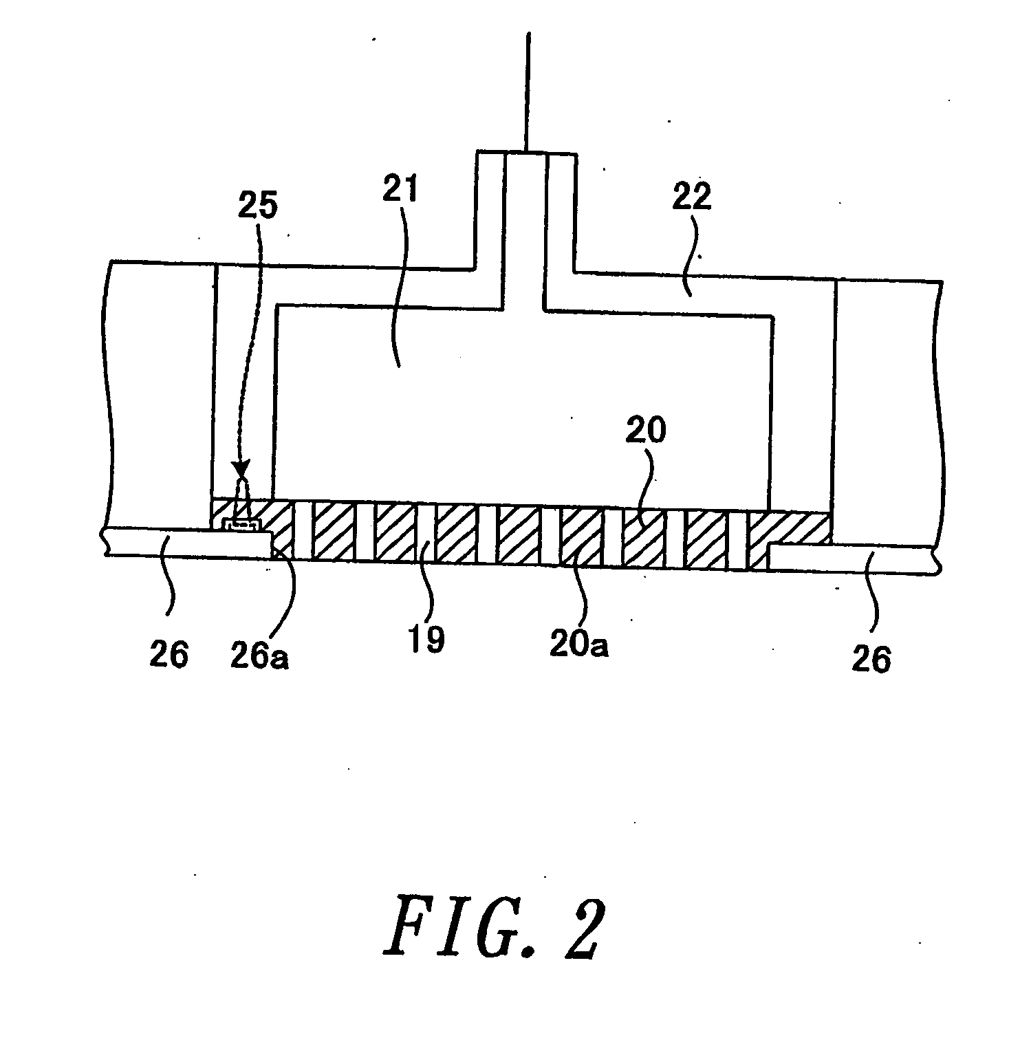
[0088]FIG. 3A shows the results of checking the pressure at individual points above the wafer W when an Ar gas is supplied into the chamber 2 via the projection type electrode plate 20. FIG. 3B shows the results when the flat electrode plate 20 which does not have the projection 20a is used. The distance between the electrode plate 20 and the susceptor 10 (gap between electrodes) was 30 mm and the Ar gas was let to flow to the surface of the wafer W of 200 mm at 300 sccm.

[0089] As shown in FIG. 3A, in the case of using the projection type electrode plate 20, the pressure above the wafer W does not change at the center portion and end portion and is nearly constant at about 1 Pa. In the case of using the flat type electrode plate 20, as shown in FIG. 2B, the pressure at the end portion above the wafer W is about 1 Pa whereas the pressure at the center portion becomes about 1.5 Pa nearly 50% higher. The pressure difference occurs near the step portion between the electrode plate 20 a...

second embodiment

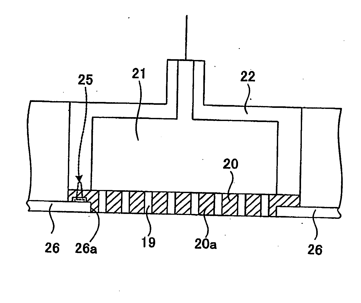
[0100] The second embodiment of the invention will be discussed below. A plasma process system 1 according to the second embodiment has nearly the same structure as the plasma process system 1 of the first embodiment illustrated in FIG. 1. FIG. 6 shows an enlarged diagram of near the upper and lower electrodes of the second embodiment. In the diagram, same reference symbols are given to those portions which are the same as those in FIGS. 1 and 2 and the description will be omitted for easier understanding.

[0101] In the second embodiment, the electrode plate 20 has a structure similar to that of the first embodiment. That is, the electrode plate 20 is formed into a projection type and the exposed surface (bottom surface) of the projection 20a and the exposed surface (bottom surface) of the shield ring 26 form approximately the same plane surface. The diameter of the opening of the focus ring 17 is set approximately equal to the diameter of the wafer W.

[0102] The ratio of the diamet...


PUM

PropertyMeasurementUnit
thicknessaaaaaaaaaa
pressureaaaaaaaaaa
frequencyaaaaaaaaaa

Abstract

That surface of an electrode plate 20 which is opposite to a susceptor 10 has a projection shape. The electrode plate 20 is fitted in an opening 26a of shield ring 26 at a projection 20a. At this time, die thickness of the projection 20a is approximately the same as the thickness of the shield ring 26. Accordingly, the electrode plate 20 and the shield ring 26 form substantially the same plane. The major surface of the projection 20a has a diameter 1.2 to 1.5 times the diameter of a wafer W. The electrode plate 20 is formed of, for example, SiC.

Description

TECHNICAL FIELD [0001] The present invention relates to a plasma process system and a plasma process method which perform processes, such as film deposition and etching, using a plasma. BACKGROUND ART [0002] A plasma process system which processes the surface of a substrate, such as a semiconductor wafer, using a plasma is used in a fabrication process for a liquid crystal display or the like. As plasma process systems, there are, for example, a plasma etching system which performs etching on a substrate and a plasma CVD system which performs chemical vapor deposition (Chemical Vapor Deposition: CVD). Of them, a parallel plate plasma process system is widely used because it has an excellent process uniformity and its system structure is relatively simple. [0003] The structure of a parallel plate plasma process system is shown in FIG. 17. As shown in FIG. 17, a plasma process system 101 comprises a chamber 102, a shower electrode 103 which feeds a process gas into the chamber 102 and...

Claims


Application Information

Patent Timeline
Patent Type & Authority Applications(United States)
IPC IPC(8): C23C16/00H01J37/32
CPCH01J37/32009H01J37/3244H01J37/32541H01L21/3065
Inventor TAKATSUKI, KOICHIYOSHITAKA, HIKARUASHIGAKI, SHIGEOINOUE, YOICHIAKAHORI, TAKASHIISHIZUKA, SHUUICHIABE, SYOICHISUZUKIKAWAMURA, KOHEIMIYOSHI, HIDENORICHUNG, GISHIOSHIMA, YASUHIROTAKAHASHI, HIROYUKI
Owner TOKYO ELECTRON LTD
Why Eureka
Try Eureka