Liquid crystal display device and method of suppressing afterimages

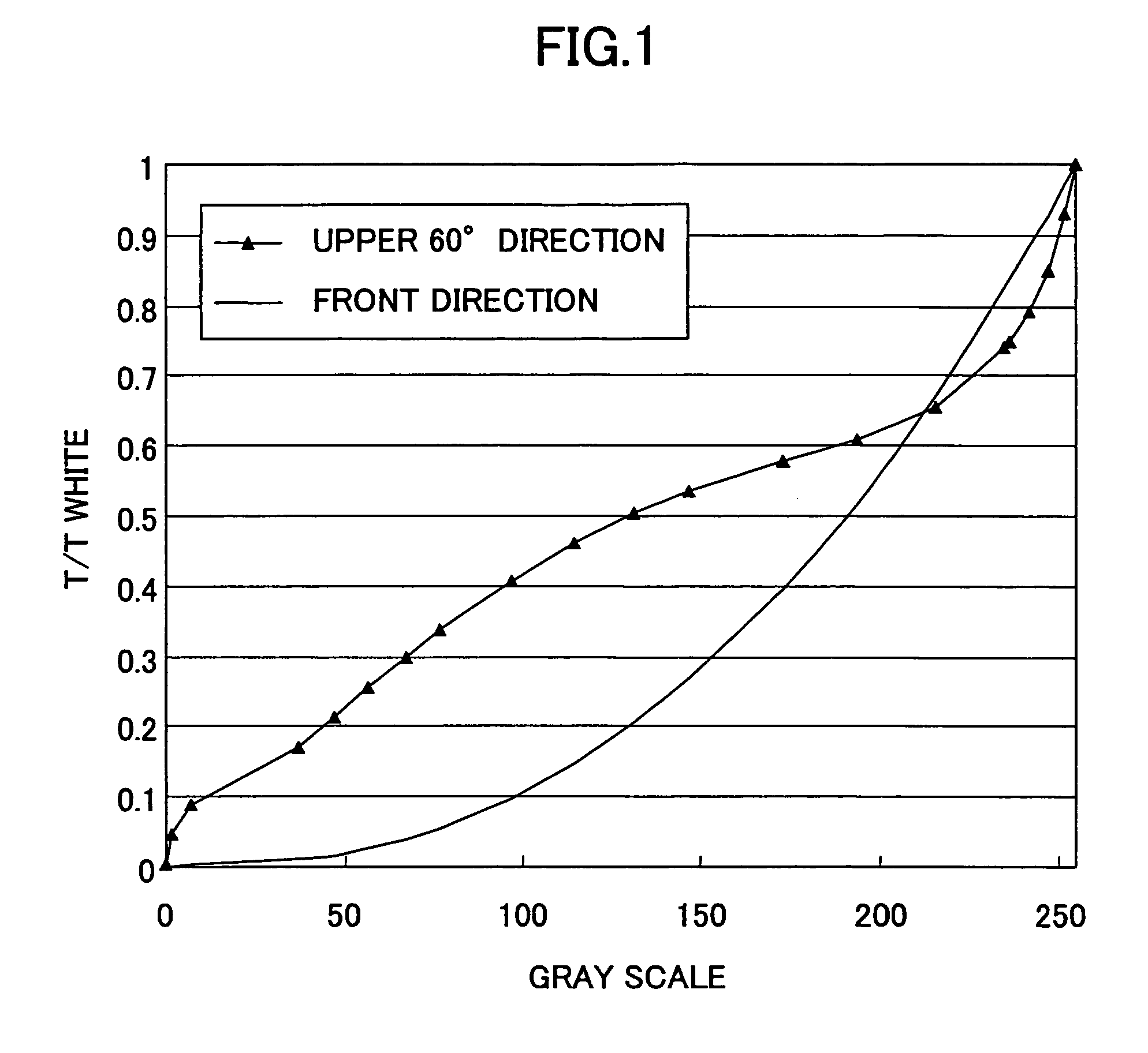
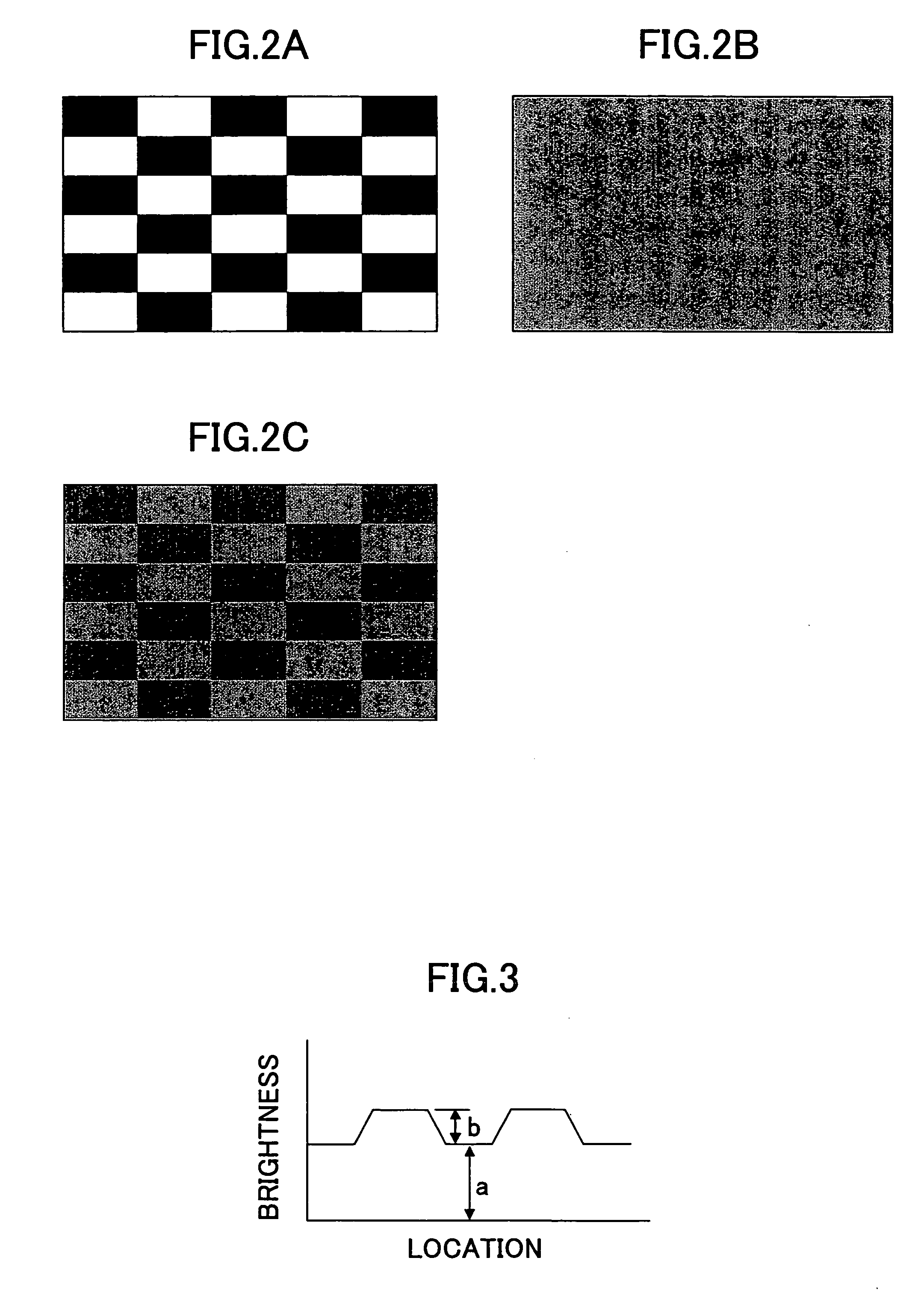
a liquid crystal display and afterimage technology, applied in static indicating devices, non-linear optics, instruments, etc., can solve the problems of remarkable change of contrast and color tone, poor viewing angle characteristics, and whitish representation

Inactive Publication Date: 2007-06-14
SHARP KK
View PDF5 Cites 6 Cited by
  • Summary
  • Abstract
  • Description
  • Claims
  • Application Information

AI Technical Summary

Benefits of technology

[0056] Thus, with the liquid crystal display device comprising: first through N-th gate bus lines formed parallel on a substrate; plural data bus lines formed over said substrate so as to cross said first through N-th gate bus lines via an insulation film; plural accumulation capacitor bus lines formed over said substrate parallel to said first through N-th gate bus lines; first and second transistors formed in each stage defined by a gate bus line and in each column defined by a data bus line, each of said first and second transistors having, in each of said stages and columns, a gate electrode connected electrically to said gate bus line and a drain electrode connected to said data bus line; a first picture element electrode connected, in each of said stages and columns, electrically to a source electrode of said first transistor; a second picture element electrode connected, in each of said stages and columns, to a source electrode of said second transistor and isolated from said first picture element electrode; and a third transistor provided in each of said stages and columns, said third transistor having, in each of said stages and columns,

Problems solved by technology

However, such a TN mode liquid crystal display device has a drawback of poor viewing angle characteristics in that there is caused a remarkable change of contrast and tone of color when the images on the liquid crystal display device is viewed from an oblique direction.
In such a conventional MVA liquid crystal display device, however, there still

Method used


Image

  • Liquid crystal display device and method of suppressing afterimages
  • Liquid crystal display device and method of suppressing afterimages
  • Liquid crystal display device and method of suppressing afterimages

Examples


first embodiment

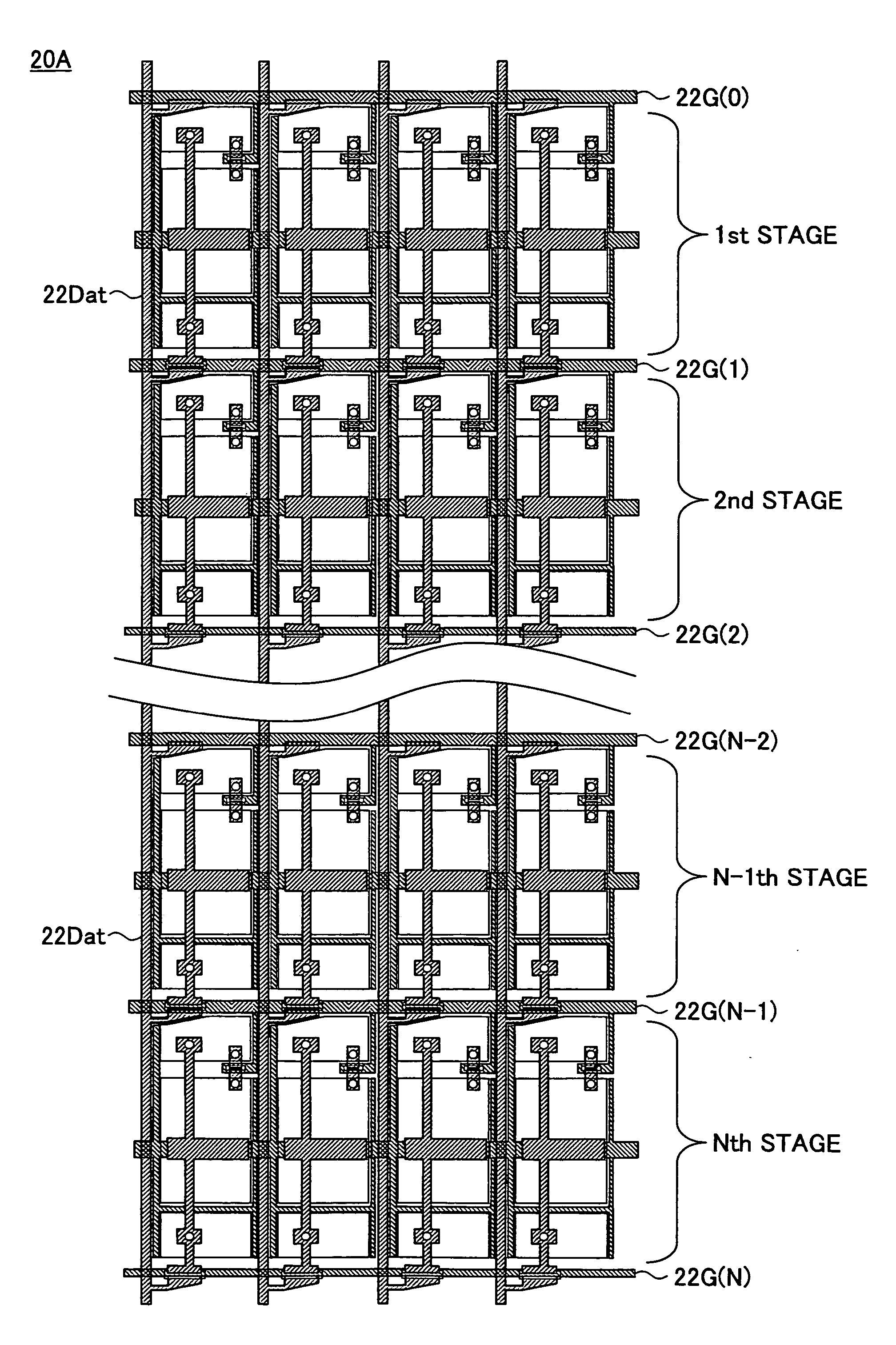
[0072]FIGS. 4A-4C are diagrams showing the construction of a liquid crystal display device 20 according to a related part of the present invention, wherein FIG. 4A shows a single picture element formed on a TFT substrate in a plan view, FIG. 4B shows a cross-sectional view of the single picture element taken along a line A-A′ of FIG. 4A, while FIG. 4C is an equivalent circuit diagram corresponding to the construction of FIGS. 4A and 4B.

[0073] Referring to the cross-sectional diagram of FIG. 4B at first, the liquid crystal display device 20 includes glass substrates 21A and 21B opposing with each other and a liquid crystal layer 22 confined therebetween, wherein there are formed a gate bus line 22 G and an accumulation capacitance bus line 22C on the glass substrate 21A.

[0074] The gate bus line 22G and the accumulation capacitance bus line 22C are covered by an insulation film 22Gox constituting a gate insulation film of a TFT 24T1, and a channel layer 22Ch of amorphous silicon or ...

second embodiment

[0093]FIG. 8 is a diagram showing the construction of a liquid crystal display device 20B according to a second embodiment of the present invention, wherein those parts corresponding to the parts decried previously are designated by the same reference numerals and the description thereof will be omitted.

[0094] The present embodiment corresponds to the case that there is little operational margin in the driver integrated circuit device. Thus, with the present embodiment, the gate bus line driven at the end of the frame and the gate bus line newly added with the present invention are connected electrically and are driven at the same time. Thus, with the embodiment of FIG. 8, the construction of the liquid crystal panel is identical with the construction of FIG. 7, and only the driving circuit is changed.

[0095] By driving the gate bus lien G(N), which is driven at the end of the frame, concurrently with the newly added gate bus line G(0), the electric charges on the floating sub-pict...

third embodiment

[0096]FIG. 9 shows the construction of a liquid crystal display device 20C according to a third embodiment of the present invention, wherein those parts corresponding to the parts described previously are designated by the same reference numerals and the description thereof will be omitted.

[0097] With the embodiment of FIG. 8, there is a need of modifying the drive circuit, and thus, there is a need of work load for modifying the circuit design.

[0098] With the present invention, a data bus line 22DatS used for connecting the newly added gate bus line G(0) and the gate bus line G(N) driven last is formed further outside of the outermost data bus line 22Dat(M). Thereby, the additional data bus line 22DatS is connected electrically to the additional gate bus line 22G(0) via a contact hole 22DatC1 and further to the last gate bus line 22G(N) via another contact hole 22DatC2.

[0099] With this, it becomes possible to suppress the burning of images by driving the newly added gate bus lin...


PUM


Abstract

A liquid crystal display device includes a gate bus line and a data bus line formed on a first substrate, a first transistor formed on the first substrate and connected to the gate bus line and the data bus line, a plurality of sub-picture element electrodes formed the said first substrate in a picture element region defined by the gate bus line and the data bus line, a control electrode formed on the first substrate in capacitance coupling with at least one of the plural sub-picture element electrodes, the control electrode being applied with a display voltage from the data bus line via the first transistor, and an auxiliary capacitance bus line held at a predetermined voltage level and constituting an auxiliary capacitance between the auxiliary capacitance bus line and the control electrode, wherein there is provided a second transistor between the sub-picture element electrode coupled with the control electrode by the capacitance coupling and the auxiliary capacitance bus line or between the sub-picture element electrode coupled with the control electrode by the capacitance coupling and the sub-picture element electrode connected to the first transistor, the second transistor being driven by a signal in a gate bus line different from the gate bus line to which the first transistor is connected, wherein there is provided a gate bus line driving solely the second transistor.

Description

BACKGROUND OF THE INVENTION [0001] The present invention generally relates to liquid crystal display devices and more particularly to a liquid crystal display device having plural sub-picture element electrodes in a single picture element region and a method of suppressing afterimages therein. Particularly, the present invention relates to a liquid crystal display device in which at least one sub-picture element electrode is coupled to a control electrode to which a display voltage is applied via capacitance and the method of suppressing afterimages, or burning of images, in such a liquid crystal display device. [0002] A liquid crystal display device has a compact size in terms of thickness as compared with CRT (cathode ray tube) and has an advantageous feature of low drive voltage and small power consumption. Thus, liquid crystal display devices are used extensively in various electronic apparatuses including television sets, laptop personal computers, desktop personal computers, P...

Claims


Application Information

Patent Timeline
IPC IPC(8): G09G3/36
CPCG02F1/133707G02F2001/133397G02F2001/134345G02F2001/134354G09G3/3648G09G2300/0426G09G2300/0447G09G2300/0876G09G2320/028G09G2320/046G02F1/133397G02F1/134345G02F1/134354
Inventor NAKANISHI, YOHEIKAMADA, TSUYOSHITSUDA, HIDEAKIYOSHIDA, HIDEFUMITASAKA, YASUTOSHISHIBASAKI, MASAKAZU
Owner SHARP KK
Why Eureka
Try Eureka