Optical scanner and image forming apparatus

Inactive Publication Date: 2007-06-14
RICOH KK
View PDF9 Cites 68 Cited by
  • Summary
  • Abstract
  • Description
  • Claims
  • Application Information

AI Technical Summary

Benefits of technology

[0023] According to one embodiment of the present invention, an optical scanner that can precisely scan a scan object surface and an image forming apparatus that can produce high-quality images are provided.
[0024]

Problems solved by technology

However, the printing speed cannot be enhanced sufficiently by these methods.
However, the relationship between the driving current and light output of semiconductor lasers changes with temperature, making it difficult to fix the light intensity of semiconductor lasers at a desired level.
Particularly, in vertical cavity surface emitting lasers, light emitting elements are spaced apart by short intervals on a single chip; therefore, the temperature rapidly changes due to light emission and light quench

Method used


Image

  • Optical scanner and image forming apparatus
  • Optical scanner and image forming apparatus
  • Optical scanner and image forming apparatus

Examples


Example

[0194] A first embodiment according to the present invention concerns a pixel forming apparatus. The pixel forming apparatus according to the first embodiment includes n light sources (n≧2) that are arranged at different positions in at least the sub scanning direction. Among the n light sources, m light sources (n≧m≧2) are used for forming one pixel.

[0195] A detailed description is given of the pixel forming apparatus according to the first embodiment.

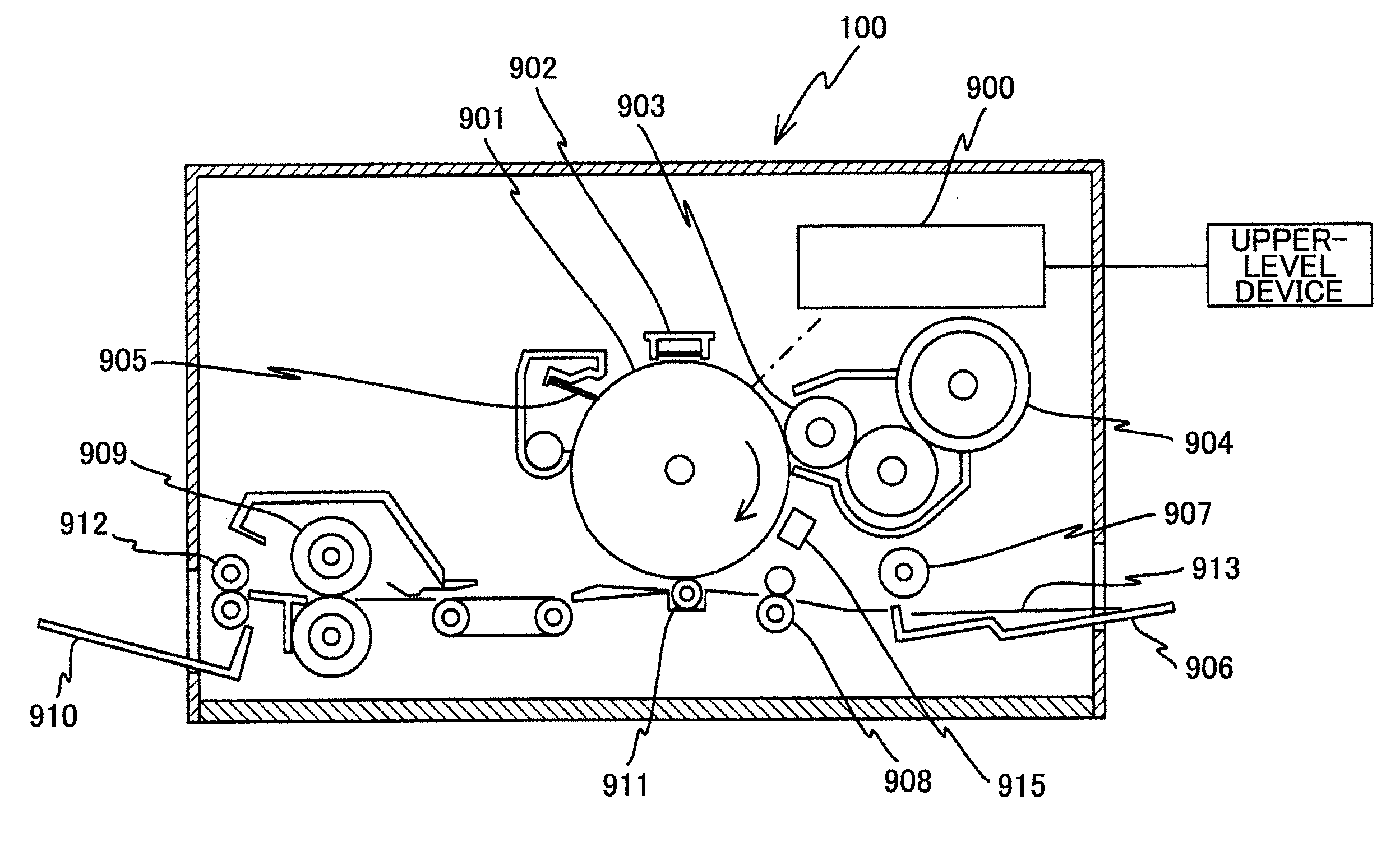
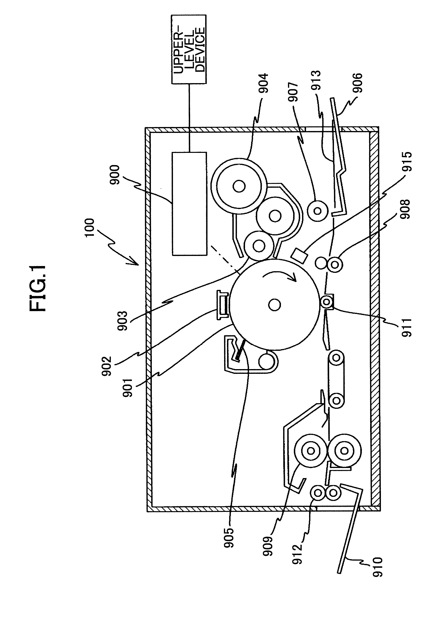
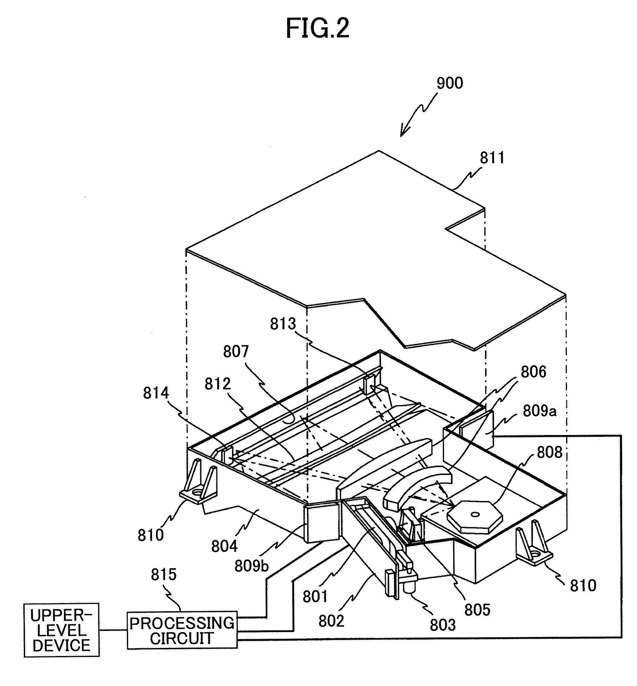
[0196] The semiconductor laser unit 1001 (hereinafter referred to as light source unit 1001) in the typical image forming apparatus (writing optical system) shown in FIG. 54 has a configuration as shown in FIG. 26. Namely, the light source unit 1001 can be a semiconductor laser array with plural light sources arranged in a lattice (plural semiconductor lasers), or a vertical cavity surface emitting laser with plural light sources arranged in a lattice on the same chip (VCSEL, vertical cavity surface emitting semiconductor laser). Th...

Example

[0199] A second embodiment according to the present invention concerns an optical scanner. The optical scanner according to the second embodiment includes n light sources (n≧2) that are arranged at different positions in at least the sub scanning direction. Among the n light sources, m light sources (n≧m≧2) are used for forming one pixel. As shown in FIG. 27, the optical scanner receives correction data for moving the centroid of one pixel in the sub scanning direction. The optical scanner includes a light source driving control unit 500 that changes the driving status of m light sources to move the centroid of a pixel in the sub scanning direction by a distance corresponding to the correction data.

[0200] More specifically, as shown in FIG. 28, the optical scanner according to the second embodiment of the present invention includes a sub scanning pixel position detecting unit 510 that detects a sub scanning pixel position and outputs correction data for correcting the pixel positio...

Example

Third Embodiment

[0229] An optical scanner according to a third embodiment of the present invention has the same configuration as those shown in FIG. 27 or 28. The optical scanner according to the third embodiment includes n light sources (n≧2) that are arranged at different positions in at least the sub scanning direction. Among the n light sources, m light sources (n≧m≧2) are used for forming one pixel. At a certain image height in the main scanning direction, one of the light sources used for emitting light is changed so that the pixel position is moved in a predetermined direction in the sub scanning direction by a distance equal to the length of the pitch of one light source. The light source driving control unit 500 according to the third embodiment changes the driving status of light sources in this manner.

[0230] The method of driving and controlling light sources according to the third embodiment is employed for a typical image that is not a line image. That is, all pixels ...


PUM


Abstract

A disclosed optical scanner includes a light source unit and a control unit configured to control the light source unit. Light emitted from the light source unit is scanned to expose a scan object surface and form an image on the scan object surface. The light source unit includes plural light sources arranged at a density equal to N (N being an integer of two or more) times higher than a density of pixels on the scan object surface. The control unit controls the light source unit such that one pixel is formed by at least two of the light sources.

Description

BACKGROUND OF THE INVENTION [0001] 1. Field of the Invention [0002] The present invention relates generally to optical scanners and image forming apparatuses, and more particularly to an optical scanner and an image forming apparatus for exposing a scan object surface by scanning a light beam to form an image. [0003] 2. Description of the Related Art [0004] In image forming apparatuses such as laser printers and digital copiers, a light beam emitted from a light source is modulated according to image information. The light beam passes through a polygon mirror and scan lenses, etc., and focuses on a photoconductor. The light beam scans the surface of the photoconductor in a predetermined direction (main scanning direction) to form a latent image (electrostatic latent image) on the photoconductor. Toner adheres to the latent image to visualize the image information. [0005]FIG. 54 is a configuration of a general image forming apparatus such as a laser printer or a digital copier employ...

Claims


Application Information

Patent Timeline
IPC IPC(8): B41J2/455
CPCB41J2/473G02B26/123G02B26/124B41J2/455
Inventor ISHIDA, MASAAKINIHEI, YASUHIROOMORI, ATSUFUMITANABE, JUN
Owner RICOH KK
Why Eureka
Try Eureka