Methods to resolve hard-to-erase condition in charge trapping non-volatile memory

Active Publication Date: 2007-06-14
MACRONIX INT CO LTD
View PDF40 Cites 7 Cited by
  • Summary
  • Abstract
  • Description
  • Claims
  • Application Information

AI Technical Summary

Benefits of technology

[0013] A method for operating a nitride trapping memory cell is provided to resolve hard-to-erase condition by employing a reset technique to eliminate or reduce the number of electrons in the middle of a junction region. When a hard-to-erase condition is detected after a series of program and erase cycles, such as 500 or 100 program and erase cycles, a substrate t

Problems solved by technology

However, the hot hole injection causes oxide damage, leading to charge loss in the high threshold cell and charge gain in the low threshold cell.
This difference in erase speed results in a large Vt distribution of the erase state, where some of the cells become hard to erase and some of them are over-erased.
Thus the target threshold Vt window is closed after many program and erase cycles and poor endurance is observed.
This phenomenon will become more serious when the technology keeps scaling down.
Evaluating the endurance and retention of a NROM array, the lack of uniformity in erase ability c

Method used


Image

  • Methods to resolve hard-to-erase condition in charge trapping non-volatile memory
  • Methods to resolve hard-to-erase condition in charge trapping non-volatile memory
  • Methods to resolve hard-to-erase condition in charge trapping non-volatile memory

Examples


Embodiment Construction

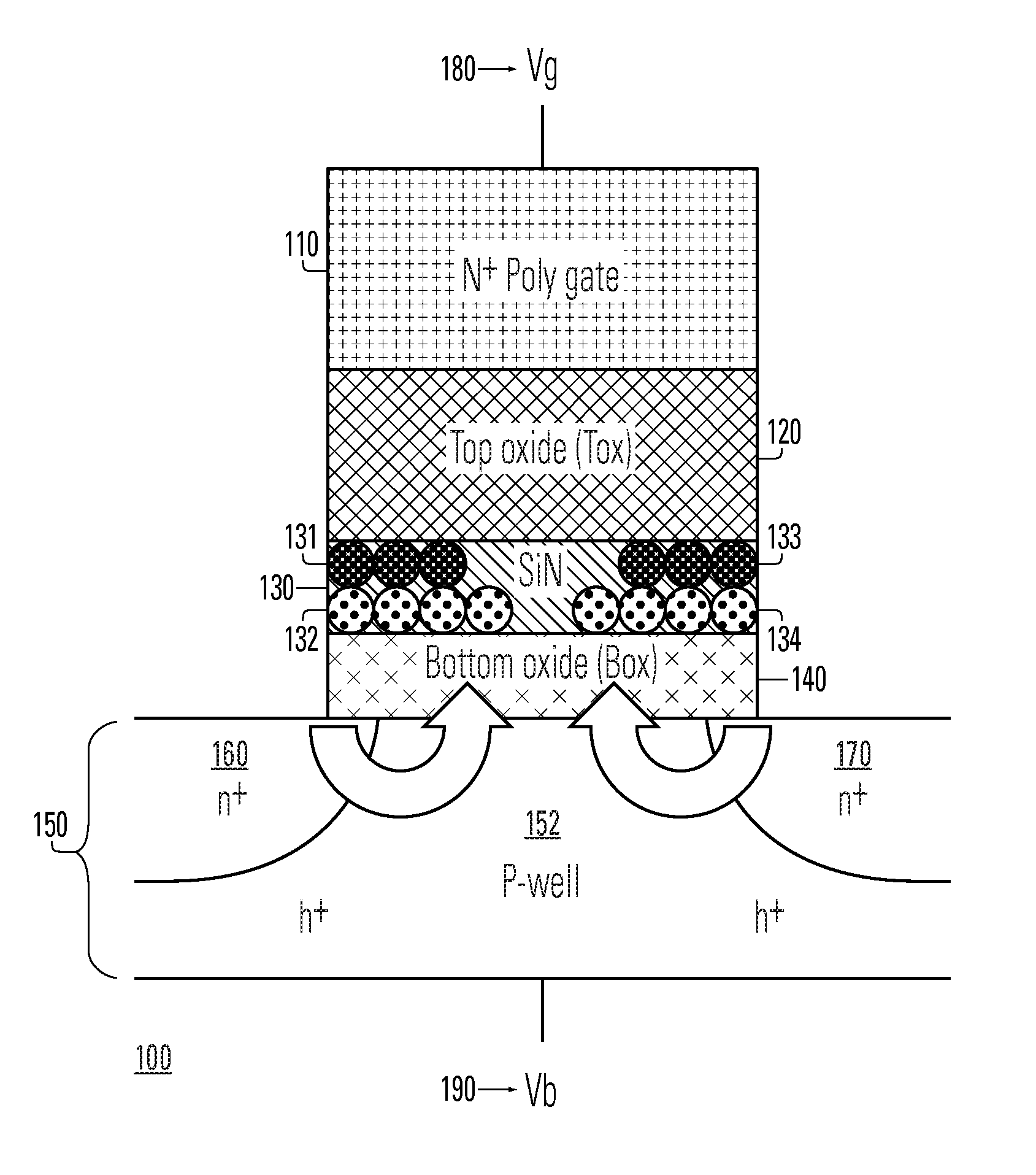
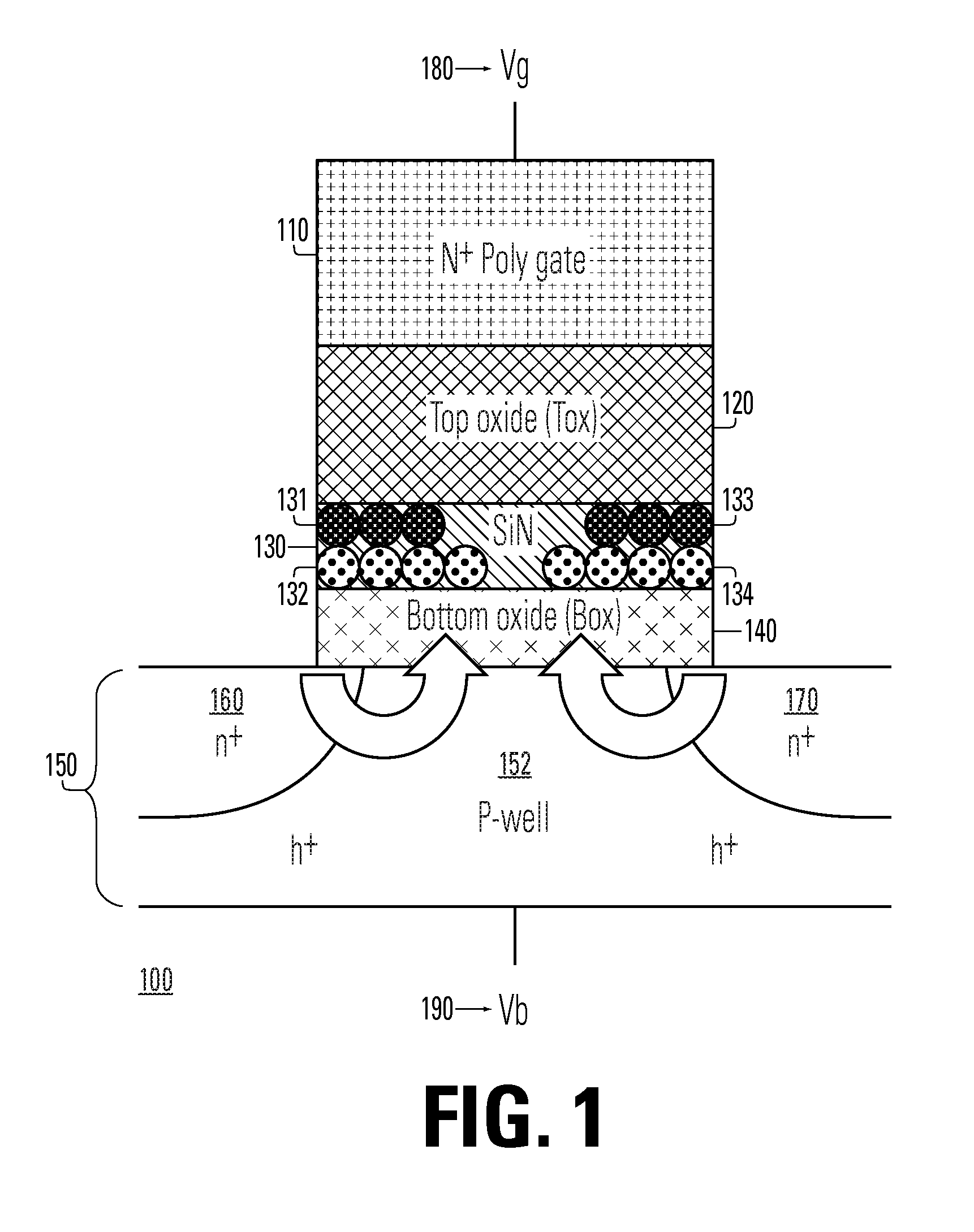
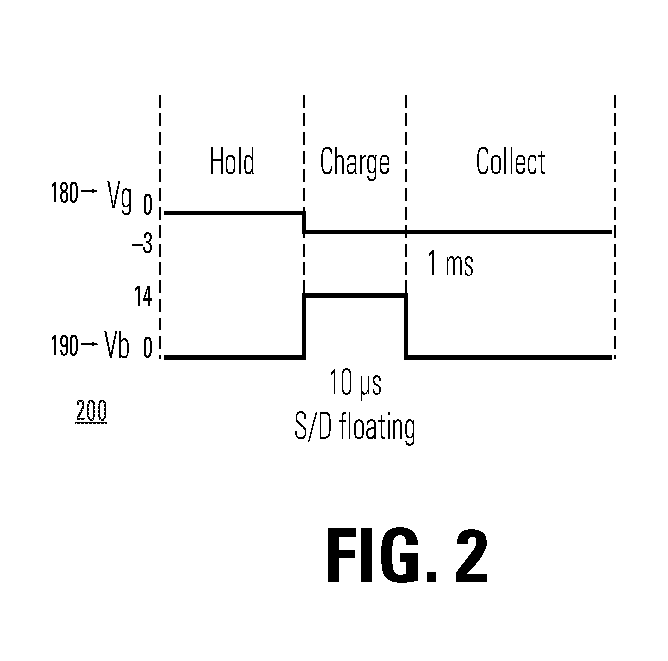
[0024] Referring now to FIG. 1, there is shown a simplified structural diagram illustrating a charge trapping memory 100 for carrying out a reset operation using a substrate transient hot hole reset (STHH) operation. The charge trapping memory cell 100 has a substrate 150 with n+ doped regions 160 and 170, and a p-doped region 152 between the n+ doped regions 160 and 170. A bottom dielectric structure 140 (bottom oxide) overlays the substrate 150, a charge trapping structure 130 (e.g. silicon nitride layer) overlays the bottom dielectric structure 140, and a top dielectric structure (top oxide) 120 overlays the charge trapping structure 130, and a N+ poly gate 110 overlays the top dielectric structure 120. A gate voltage 180, Vg, is applied to the n+ poly gate 110, and a body voltage 190, Vb, is applied to the P-well substrate 150. Representative top dielectrics include silicon dioxide and silicon oxynitride having a thickness of about 5 to 10 nanometers, or other similar high diele...


PUM


Abstract

A method for operating a nitride trapping memory cell is provided to resolve hard-to-erase condition by employing a reset technique to eliminate or reduce the number of electrons in the middle of a junction region. When a hard-to-erase condition is detected after a series of program and erase cycles, such as 500 or 100 program and erase cycles, a substrate transient hot hole (STHH) reset operation is applied. The substrate transient hot hole reset injects holes that are far away junction than band-to-band tunneling hot hole (BTBTHH) injection such that the STHH reset on cycle endurance is able to maintain a desirable cycle window to eliminate or reduce the hard-to erase condition in subsequent program and erase cycles.

Description

BACKGROUND OF THE INVENTION [0001] 1. Field of the Invention [0002] The present invention relates generally to electrically programmable and erasable memory, and more particularly, to resolve hard-to-erase condition under high cycle endurance in charge trapping memory. [0003] 2. Description of Related Art [0004] Electrically programmable and erasable non-volatile memory technologies based on charge storage structures known as Electrically Erasable Programmable Read-Only Memory (EEPROM) and flash memory are used in a variety of modem applications. A flash memory is designed with an array of memory cells that can be independently programmed and read. Sense amplifiers in a flash memory are used to determine the data value or values stored in a non-volatile memory. In a typical sensing scheme, an electrical current through the memory cell being sensed is compared to a reference current by a current sense amplifier. [0005] A number of memory cell structures are used for EEPROM and flash ...

Claims


Application Information

Patent Timeline
IPC IPC(8): G11C16/04
CPCG11C16/0475
Inventor HSU, TZU-HSUANSHIH, YEN-HAO
Owner MACRONIX INT CO LTD
Why Eureka
Try Eureka