

Semiconductor memory device
a memory device and semiconductor technology, applied in the field of sram circuit technology, can solve the problems of increasing the random variance of transistor characteristics caused by random variance in tr characteristics, serious problems, and difficulty in producing devices with good cell characteristics in the mbit order, so as to avoid the effect of reducing the yield
- Summary
- Abstract
- Description
- Claims
- Application Information
AI Technical Summary
Benefits of technology
Problems solved by technology
Method used
Image

Examples
first embodiment
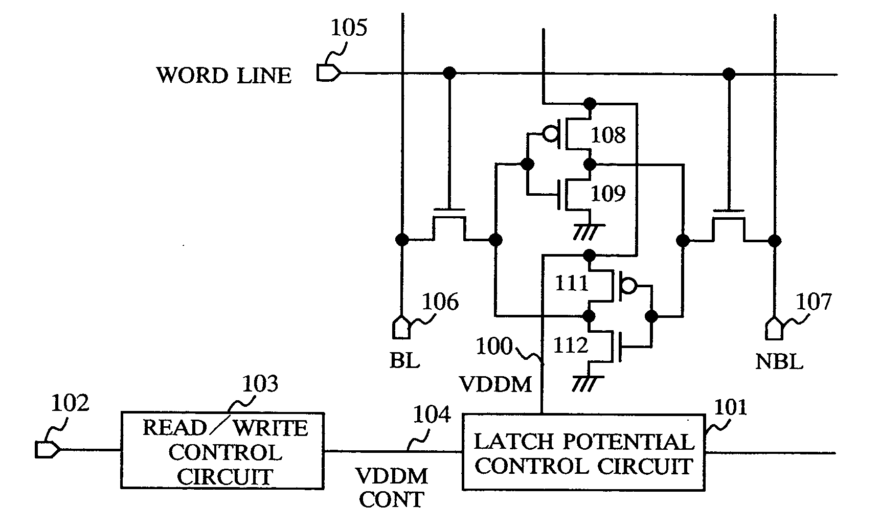
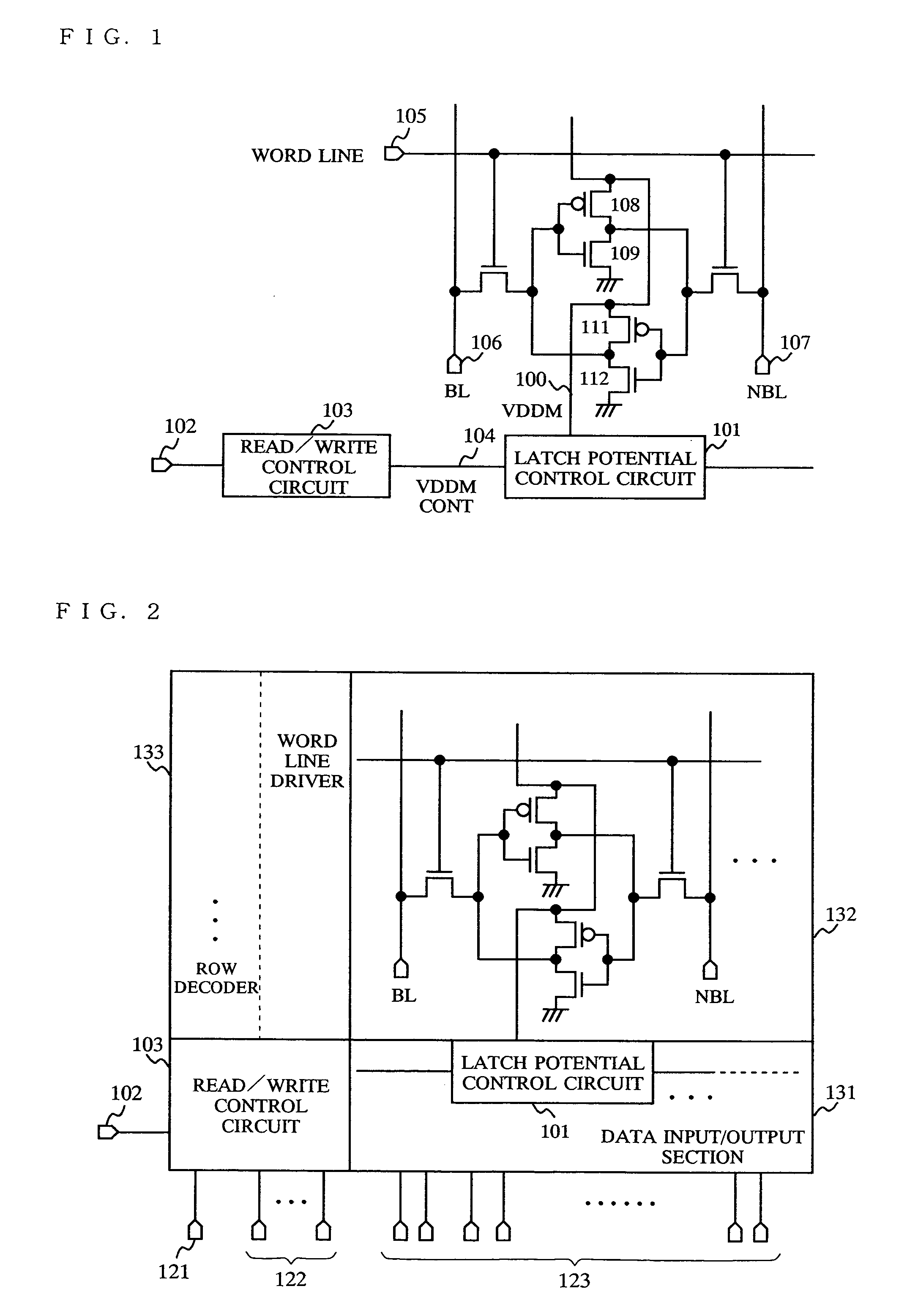
[0054] A semiconductor memory device according to a first embodiment of the present invention will be described with reference to FIG. 1 through FIG. 3, FIG. 13 and FIG. 19. In the first embodiment, a technology for VDDM control will be described, which mainly corresponds to claims 1, 9 and 16. In this embodiment, for example, in order to prevent over-time deterioration caused by static noise margin (SNM) described above, a test mode setting pin 102 is provided so that a test mode which is different from a normal operation mode can be set. The power supply potential is controlled to reduce the SNM, and thus a state which has an SNM value equivalent to, or lower than, the SNM value after the over-time deterioration is created for inspection.
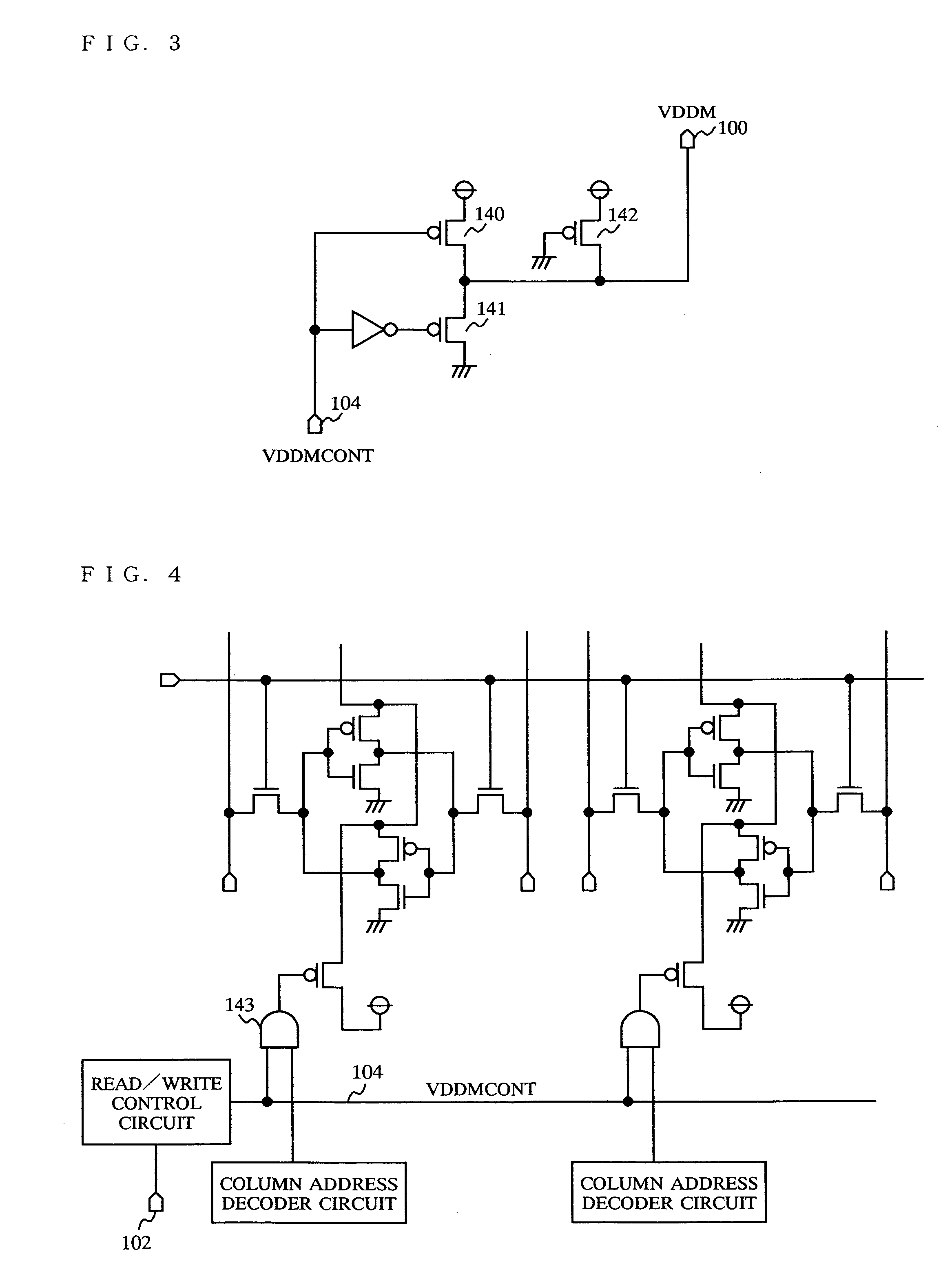
[0055] First, a technology for controlling the inverter latch power supply corresponding to claim 1 will be described. FIG. 1 shows a main circuit configuration of a semiconductor memory device according to the first embodiment of the present inv...
second embodiment
[0065] A semiconductor memory device according to a second embodiment of the present invention will be described with reference to FIG. 4 and FIG. 8. In the second embodiment, a technology for VDDM cutoff will be described, which mainly corresponds to claims 2, 7 and 8.
[0066] During the read operation in the test mode, an SNM stress mode can be created by setting the VDDM 100 at a certain potential using the circuit in FIG. 3. Alternatively, as shown in FIG. 4, an SNM stress mode can be created by cutting off the power supply to the VDDM 100 at the inverter latch potential, using a cutoff Tr. This VDDM cutoff technique, which uses a small number of devices and does not need a through-current component for obtaining a potential, is advantageous in consuming a very low magnitude of current, despite that it is more difficult to obtain an intended potential as compared to the first embodiment. This VDDM cutoff technique is realized by claim 2.
[0067] The control circuit for the VDDM 10...
third embodiment
[0068] A semiconductor memory device according to a third embodiment of the present invention will be described with reference to FIG. 5 through FIG. 8. In the third embodiment, a technology for boosting the voltage of word line and boosting the voltage of the bit lines will be described, which mainly corresponds to claims 3 and 4.
[0069] As shown in FIG. 5, the memory cell is provided with a potential 201 for the normal operation mode and also with as lightly higher potential 202 for the test mode. FIG. 6 shows an exemplary configuration of a word line driver 203. The test mode setting pin 102 is set to a Low potential in the normal operation mode and to a High potential in the test mode. When the potential of the test mode setting pin 102 becomes High, a Pch Tr 205 is cut off and the potential 201 for the normal operation mode is prevented from being supplied. Instead, a Pch Tr 206 is placed into an ON state and the potential 202 for the test mode is supplied. When the potential o...
PUM
 Abstract
Description
Claims
Application Information