Semiconductor manufacturing apparatus and semiconductor manufacturing method using the same

a manufacturing apparatus and semiconductor technology, applied in lighting and heating apparatus, charging manipulation, furniture, etc., can solve the problems of reducing the conveyance precision, affecting the accuracy of the conveyance, and affecting the contacting portion with respect to the device main body, etc., to achieve simple conveying mechanism, simple configuration, and satisfactory precision

Inactive Publication Date: 2007-06-21
SHARP KK
View PDF4 Cites 17 Cited by
  • Summary
  • Abstract
  • Description
  • Claims
  • Application Information

AI Technical Summary

Benefits of technology

[0017] According to the present invention, since the gas is emitted from the gas emission holes of the guide plate of one or the other vacuum chambers and the conveying arm is capable of moving the tray in one vacuum chamber, which is in the floated state by the emitted gas, from the guide plate of one vacuum chamber to the guide plate of the other vacuum chamber along the guide plate when the conveying arm moves the tray, the movable portion or the drive portion necessary for conveying the substrate is reduced as much as possible, and the substrate is conveyed at satisfactory precision with a simple configuration. Further, by arranging the conveying arm in one of the two adjacent vacuum chambers, a transfer chamber for temporarily accommodating the conveying robot or the substrate before input and the like becomes unnecessary.
[0018] That is, the conveying mechanism is simple, and the conveyance drive section is not necessary in the vacuum chamber, whereby various problems of the substrate processing device pertaining to the in-line conveying method and the feed conveying method of the prior art are resolved, that is, complication of the structure of the apparatus and increase in cost resulting therefrom, lowering of cleanliness in the vacuum chamber caused by the conveyance drive section, grounding of the tray, lowering of conveyance precision, and increase in device installation area.

Problems solved by technology

Since the tray is held with the wheel, bearing or the like, the contacting portion with respect to the device main body is limited, and grounding of the tray becomes a problem when using a high frequency power supply and the like.
If heating is involved in the manufacturing step of the semiconductor device, a certain degree of clearance must be provided in consideration of thermal expansion caused by heating in order for the drive portion such as chain, toothed gear or the like to continue to appropriately function around the time of heating, but such clearance may possibly lower the conveyance precision.
Countermeasures have been proposed such as configuring the drive portion with a material of small thermal expansion or suppressing thermal expansion by cooling the drive portion, but the cost increases or the structure of the apparatus becomes complicating in either case.
Further, with regards to the positioning of the tray, a detector for accurately detecting the position of the tray, and an actuator or a driving device of high precision for stopping the tray at a predetermined position at satisfactory precision are required, which increases cost and complicates the structure of the apparatus.
Further, an image recognizing device or other positioning mechanisms must be used to perform positioning of the substrate to be conveyed, which increases the cost and complicates the structure of the apparatus.

Method used


Image

  • Semiconductor manufacturing apparatus and semiconductor manufacturing method using the same
  • Semiconductor manufacturing apparatus and semiconductor manufacturing method using the same
  • Semiconductor manufacturing apparatus and semiconductor manufacturing method using the same

Examples


embodiment 1

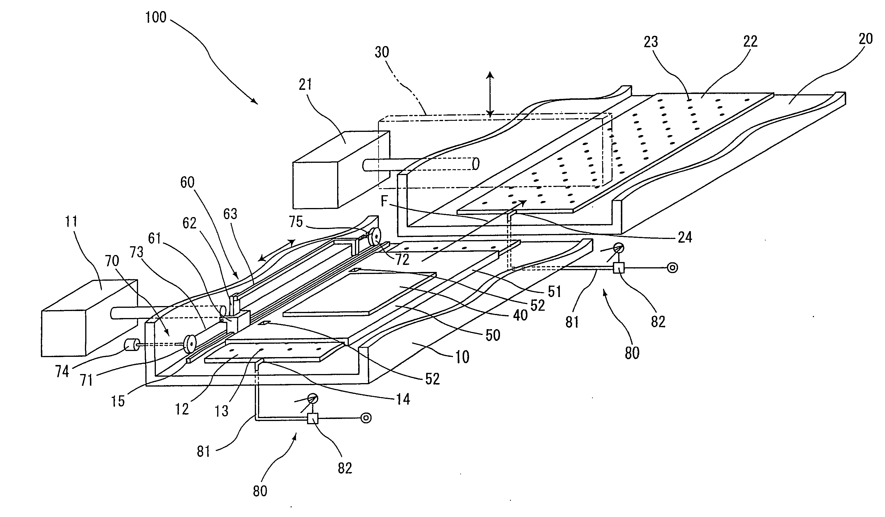
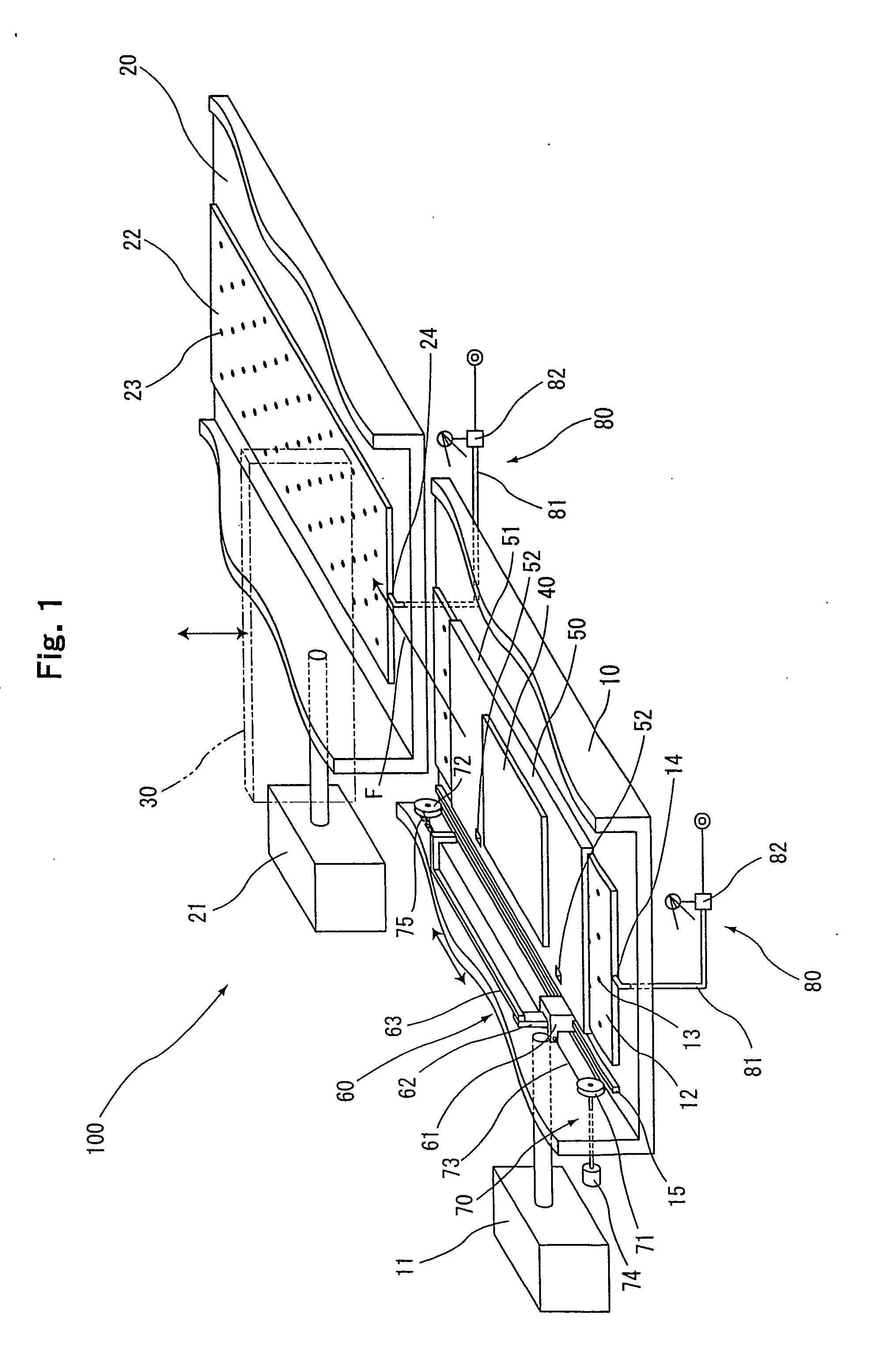
[0071] The semiconductor manufacturing apparatus according to embodiment 1 of the present invention will now be explained based on FIGS. 1 to 11, and FIG. 15.

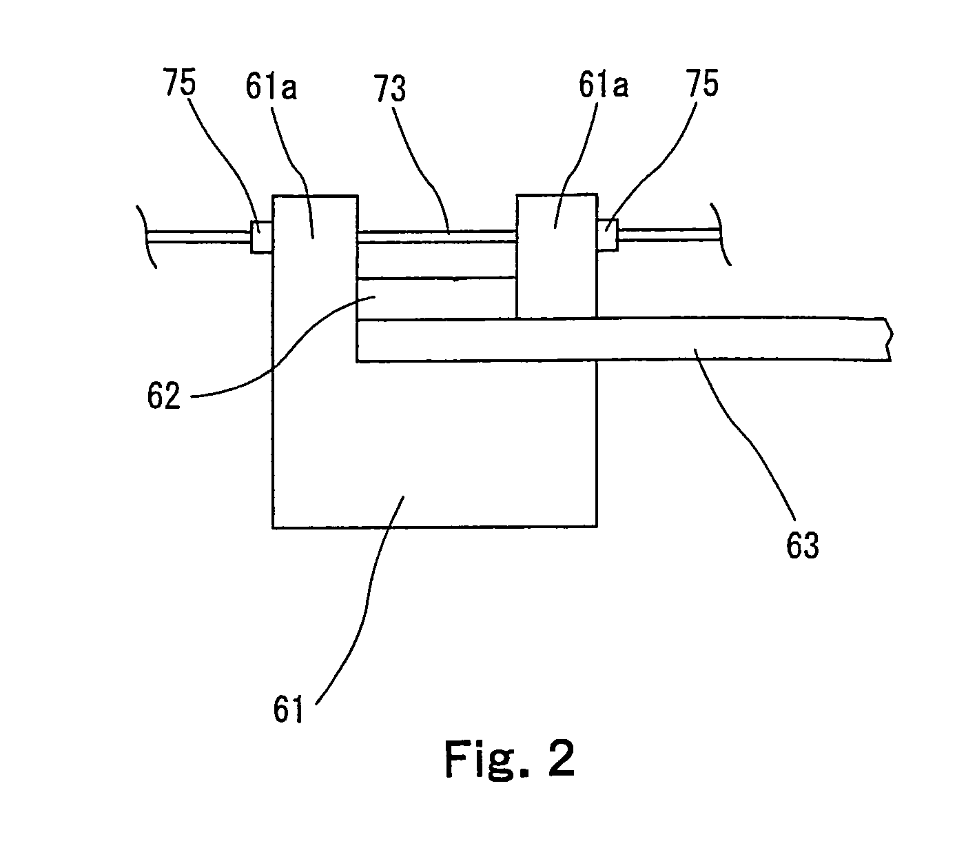
[0072]FIG. 1 is a perspective view of a semiconductor manufacturing apparatus according to embodiment 1, FIG. 2 is a partially enlarged view of the semiconductor manufacturing apparatus shown in FIG. 1, and FIG. 3 to FIG. 11 are explanatory views for explaining the method for moving the plate of the semiconductor manufacturing apparatus shown in FIG. 1. FIG. 15 is a schematic configuration view of the semiconductor manufacturing apparatus shown in FIG. 1. In FIG. 1 and FIG. 15 showing the configuration of the semiconductor manufacturing apparatus of the present invention, the processing section that performs the processes necessary for manufacturing the semiconductor device is omitted.

[0073] As shown in FIG. 1, the semiconductor manufacturing apparatus 100 according to embodiment 1 includes first and second vacuum chambers 10...

embodiment 2

[0115] Embodiment 2 of the present invention will now be explained based on FIG. 12. FIG. 12 is a perspective view of a semiconductor manufacturing apparatus according to embodiment 2.

[0116] As shown in FIG. 12, the semiconductor manufacturing apparatus 200 according to embodiment 2 has a third vacuum chamber 230 added to the semiconductor manufacturing apparatus 100 (see FIG. 1) of embodiment 1.

[0117] The third vacuum chamber 230 has substantially the same configuration as the first vacuum chamber 210, and only the attaching direction of the arm portion 263 with respect to the arm guide 262 of the conveying arm 260 differs from that of the first vacuum chamber 210. Other configurations are the same as the semiconductor manufacturing apparatus 100 of embodiment 1.

[0118] The chamber pressure control of when conveying the tray from the second vacuum chamber 220 to the third vacuum chamber 230 is the same as in embodiment 1.

embodiment 3

[0119] Embodiment 3 of the present invention will now be explained based on FIG. 13. FIG. 13 is a perspective view of a semiconductor manufacturing apparatus according to embodiment 3.

[0120] As shown in FIG. 13, the semiconductor manufacturing apparatus 300 according to embodiment 3 has a third vacuum chamber 330 and a fourth vacuum chamber 340 added to the semiconductor manufacturing apparatus 100 (see FIG. 1) of embodiment 1. Accompanied therewith, the rails 335a, 335b, the conveying arms 360a, 360b and the drive sections 370a, 370b are arranged on both sides of the guide plate 332 in the third vacuum chamber of embodiment 3.

[0121] The conveying arm 360a functions to convey the tray 350 between the second vacuum chamber 320 and the third vacuum chamber 330, and the conveying arm 360b functions to convey the tray 350 between the third vacuum chamber 330 and the fourth vacuum chamber 340. Thus, the attaching directions of the arm portions 363a, 363b with respect to the arm guides ...


PUM

PropertyMeasurementUnit
diameteraaaaaaaaaa
diameteraaaaaaaaaa
distanceaaaaaaaaaa

Abstract

A semiconductor manufacturing apparatus comprising: a plurality of vacuum chambers corresponding to a plurality of processing sections necessary for manufacturing a semiconductor device; an exhaust device connected to each vacuum chamber; a plate shaped guide plate arranged at the bottom of each vacuum chamber and having a plurality of gas emission holes; and a gas supply source for supplying gas to the gas emission holes, wherein the plurality of vacuum chambers are adjacent to each other by way of a shutter, one of the two adjacent vacuum chambers includes a tray mounted on the guide plate for mounting a substrate to be performed with a predetermined process, a conveying function section having a conveying arm for moving the tray from one vacuum chamber to the other vacuum chamber along the guide plate, and a controlling function section, the controlling function section performing the control so as to open the shutter to communicate the two adjacent vacuum chambers, emit gas from the gas emission holes of the guide plate of the vacuum chambers, and move the tray in one vacuum chamber, which is floated by the emitted gas, from the guide plate of one vacuum chamber to the guide plate of the other vacuum chamber along the guide plate by means of the conveying arm.

Description

TECHNICAL FIELD [0001] The present invention relates to a semiconductor manufacturing apparatus and a semiconductor manufacturing method using the same, and more particularly to a semiconductor manufacturing apparatus including a plurality of vacuum chambers adjacent to each other, which correspond to a plurality of processing sections necessary for manufacturing a semiconductor device, and a semiconductor manufacturing method using the same. BACKGROUND ART [0002] A semiconductor manufacturing apparatus that employs a vacuum chamber is generally used when manufacturing a semiconductor thin film on a substrate. [0003] Such a semiconductor manufacturing apparatus generally includes a plurality of vacuum chambers with a processing function necessary for manufacturing the semiconductor device such as film growing, and a conveying mechanism for conveying the substrate to be performed with the semiconductor manufacturing process between a plurality of vacuum chambers. [0004] An in-line ty...

Claims


Application Information

Patent Timeline
Patent Type & Authority Applications(United States)
IPC IPC(8): C23C16/00B65H1/00B65G49/06H01L21/677
CPCB65G49/061B65G49/065B65G2249/02B65G2249/04H01L21/67748H01L21/67784Y10S414/135
Inventor FUKUOKA, YUSUKEKISHIMO, KATSUSHI
Owner SHARP KK
Why Eureka
Try Eureka