Method of manufacturing flexible wiring substrate and method of manufacturing electronic component mounting structure

a technology of flexible wiring and mounting structure, which is applied in the direction of printed circuit manufacturing, printed circuit aspects, non-metallic protective coating applications, etc., can solve the problems of difficult to form via holes and wiring patterns, extreme technical difficulties, etc., and achieve simple transportation and handling of substrates, easy to respond, and good reliability

Inactive Publication Date: 2007-06-21
SHINKO ELECTRIC IND CO LTD
View PDF8 Cites 23 Cited by
  • Summary
  • Abstract
  • Description
  • Claims
  • Application Information

AI Technical Summary

Benefits of technology

[0022]When the electronic component is mounted on the flexible wiring substrate according to the present invention, the electronic component (semiconductor chip) can be connected and mounted onto the uppermost layer of the built-up wiring layer in a state that the reinforcing metal layer is provided on the overall back surface. Then, the reinforcing metal layer is patterned or removed. According to such steps, the s

Problems solved by technology

Therefore, it is difficult to form the via hole and the wiring pattern at a fine pitch (for example, 30 μm pitch (line

Method used


Image

  • Method of manufacturing flexible wiring substrate and method of manufacturing electronic component mounting structure
  • Method of manufacturing flexible wiring substrate and method of manufacturing electronic component mounting structure
  • Method of manufacturing flexible wiring substrate and method of manufacturing electronic component mounting structure

Examples


first embodiment

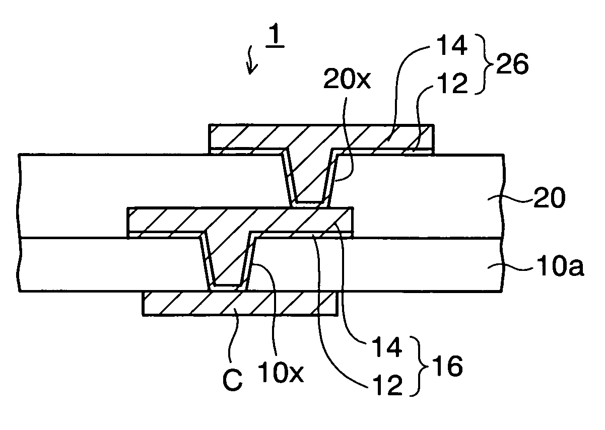
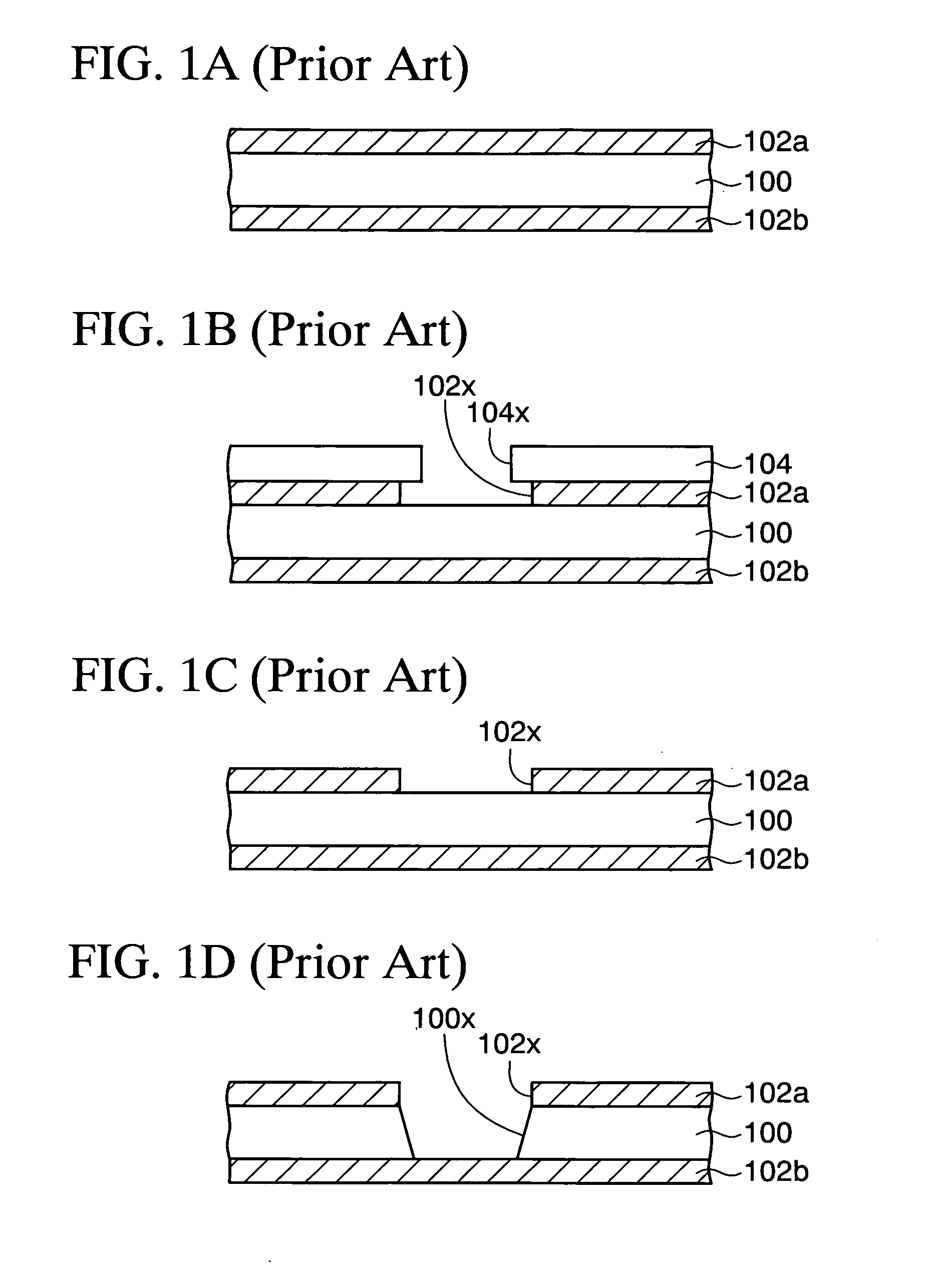
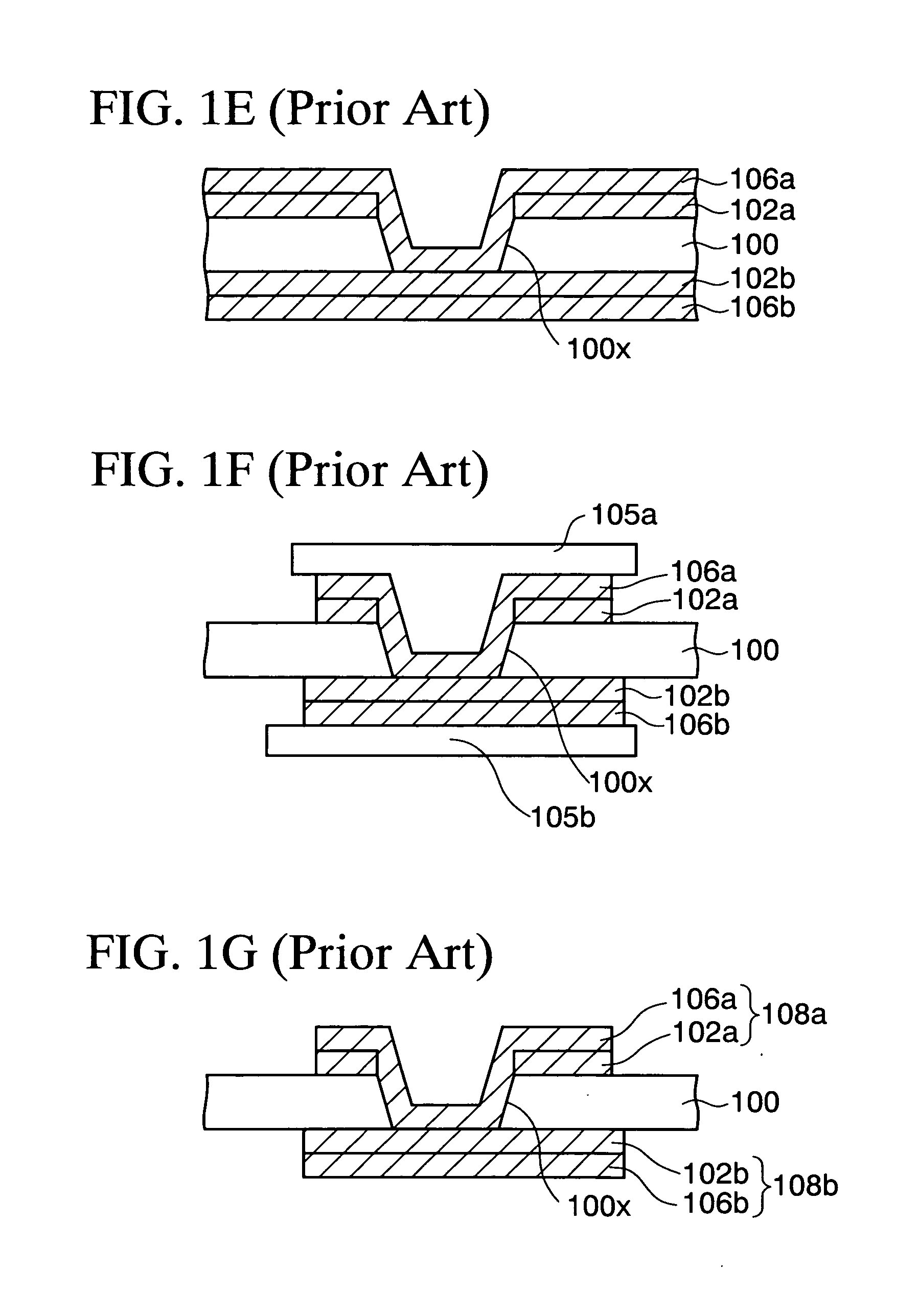
[0032]FIGS. 2A to 2I are sectional views showing a method of manufacturing a flexible wiring substrate according to a first embodiment of the present invention. In a method of manufacturing a flexible wiring substrate according to the first embodiment of the present invention, as shown in an upper view of FIG. 2A, first, a long tape-like substrate 10 which is pulled out from a reel (winding member) 5 and is carried in the longitudinal direction is prepared. As shown in a lower view of FIG. 2A, the tape-like substrate 10 is composed of a resin layer 10a and a reinforcing metal layer 10b provided on a lower surface of the resin layer 10a. For example, the resin layer 10a is formed of a polyimide layer whose film thickness is about 25 μm, and the reinforcing metal layer 10b is formed of a copper foil whose film thickness is 15 to 18 μm.

[0033]The tape-like substrate 10 is pulled out from the reel 5 and is carried into various manufacturing systems 7 (reel-to-reel system) in a state that...

second embodiment

[0057]FIGS. 4A to 4C are sectional views showing a method of manufacturing a first electronic component mounting structure according to a second embodiment of the present invention. In the second embodiment, a mode where an electronic component is mounted on the flexible wiring substrate will be explained hereunder, on the base of the technical idea of the manufacturing method of the flexible wiring substrate of the present invention. In the second embodiment, the same reference numerals are affixed to the same elements as the first embodiment and their explanation will be omitted herein.

[0058]First, as shown in FIG. 4A, the predetermined built-up wiring layer is formed on the tape-like substrate 10 by the similar method to the first embodiment. In FIG. 4A, like the first embodiment, an example where the first and second wiring patterns 16, 26 are stacked on the tape-like substrate 10 is illustrated. Then, a solder resist film 22 in which an opening portion 22x is provided on the co...


PUM


Abstract

A method of manufacturing a flexible wiring substrate of the present invention includes the steps of preparing a tape-like substrate composed of a resin layer and a reinforcing metal layer provided on its lower surface, then forming a via hole whose depth reaches the reinforcing metal layer by processing the resin layer of the tape-like substrate by the laser, and then forming a wiring pattern which is connected to the reinforcing metal layer through the via hole on the resin layer by the semi-additive process, wherein the reinforcing metal layer is patterned to constitute a connection pad connected to the wiring pattern or is removed.

Description

CROSS-REFERENCE TO RELATED APPLICATIONS[0001]This application is based on and claims priority of Japanese Patent Application No. 2005-366491 filed on Dec. 20, 2005, the entire contents of which are incorporated herein by reference.BACKGROUND OF THE INVENTION[0002]1. Field of the Invention[0003]The present invention relates to a method of manufacturing a flexible wiring substrate and a method of manufacturing an electronic component mounting structure and, more particularly, the method of manufacturing the flexible wiring substrate that is applicable to a tape package such as a tape BGA, a tape CSP, or the like, and the method of manufacturing the electronic component mounting structure for mounting an electronic component onto the wiring substrate.[0004]2. Description of the Related Art[0005]In the prior art, there are the tape packages such as the tape BGA (Ball Grid Array), the tape CSP (Chip Size Package), etc. using the polyimide tape as the substrate. In an example of a method ...

Claims


Application Information

Patent Timeline
IPC IPC(8): H01L21/00
CPCH01L21/486H01L23/3121H01L23/4985H01L2924/19041H05K1/0393H05K3/108H05K3/205H05K3/28H05K3/4007H05K3/421H05K3/4644H05K2201/0367H05K2201/0394H05K2201/09563H05K2203/0384H01L2224/48227H01L2224/16225H01L2224/48228H05K3/30
Inventor NOMURA, TOMOHIRO
Owner SHINKO ELECTRIC IND CO LTD
Why Eureka
Try Eureka