Method for manufacturing field effect transistor having channel consisting of silicon fins and silicon body and transistor structure manufactured thereby

a technology of field effect transistor and silicon body, which is applied in the direction of basic electric elements, semiconductor devices, electrical devices, etc., can solve the problems of difficult to control the exact height of the silicon channel, complicated to correct the device channel width in the device layout, so as to achieve the effect of increasing the current value and simply correcting the channel width

Inactive Publication Date: 2007-06-21
KOREA ADVANCED INST OF SCI & TECH
View PDF1 Cites 22 Cited by
  • Summary
  • Abstract
  • Description
  • Claims
  • Application Information

AI Technical Summary

Benefits of technology

[0040] Another object of the present invention is to provide a field effect transistor manufactured by said manufacturing method, which has increased current value and can be simply corrected for the channel width in the device layout.
[0041] To achieve the above objects, according to a first embodiment, the present invention provides a method for manufacturing a field effect transistor having a channel consisting of silicon fins and a silicon body, the method comprising the steps of: (a) forming a hard mask pattern on a substrate comprising a silicon thin film; (b) anisotropically etching the silicon thin film to a predetermined thickness using the mask pattern as a mask so as not only to form silicon fins where a channel is to be formed and a silicon pattern where a source / drain region is to be formed, but also to form a silicon body that connects the silicon fins to each other to form a channel; (c) partially etching the silicon thin film using an active mask so as to isolate the source / drain region and the device from each other; and (d) growing a gate dielectric film around the silicon channel and sequentially depositing a gate material and a gate mask on the resulting structure, followed by forming a gate region.
[0042] According to a second embodiment, the present invention provides a method for manufacturing a field effect transistor having a channel consisting of silicon fins and a silicon body, the method comprising the steps of: (a) forming a hard mask pattern on a substrate comprising a silicon thin film; (b) partially etching the silicon thin film using an active mask so as to isolate a source / drain region and the device from each other; (c) anisotropically etching the silicon thin film to a predetermined thickness using the mask pattern as a mask so as not only to form silicon fins where a channel is to be formed and a silicon pattern where a source / drain region is to be formed, but also to form a silicon body that connects the silicon fins to each other to form the channel; (d) growing a gate dielectric film around the silicon channel and sequentially depositing a gate material and a gate mask on the resulting structure, followed by forming a gate region. portions where silicon fins are to be formed; (d) forming silicon fins on said formed portions by selective epitaxial growth of silicon; and (e) growing a gate dielectric film around the silicon channel and sequentially depositing a gate material and a gate mask on the resulting structure, followed by forming a gate region.
[0043] According to a fifth embodiment, the present invention provides a method for manufacturing a field effect transistor having a channel consisting of silicon fins and a silicon body, the method comprising the steps of: (a) forming a substrate comprising a silicon thin film; (b) forming a hard mask on the silicon thin film, forming on the hard mask a polysilicon pattern, depositing on the resulting structure a film made of a material having a high etch selectivity, followed by etching the high etch selectivity film to form sidewalls on both sides of the polysilicon pattern; (c) etching the hard mask, the polysilicon and the silicon thin film to expose a buried oxide film so as to isolate the sidewalls as masks for forming silicon fins and the device from each other; (d) using the sidewalls and the hard mask to anisotropically etch the silicon thin film to form silicon fins where a channel is to be formed, while controlling the etching thickness of the silicon thin film to leave a thin silicon body between the silicon fins; and (e) growing a gate dielectric film around the silicon channel and sequentially depositing a gate material and a gate mask on the resulting structure, followed by forming a gate region.
[0044] According to a sixth embodiment, the present invention provides a method for manufacturing a field effect transistor having a channel consisting of silicon fins and a silicon body, the method comprising the steps of: (a) forming a substrate comprising a silicon thin film; (b) forming a hard mask on the silicon thin film, forming on the hard mask a polysilicon pattern, depositing on the resulting structure a film made of a material having a high etch selectivity, followed by etching the high etch selectivity film to form sidewalls on the polysilicon pattern; (c) etching the hard mask, the polysilicon and the silicon thin film to expose a buried oxide film so as to isolate the sidewalls as masks for forming silicon fins and the device from each other; (d) using the sidewalls and the hard mask to anisotropically etch the silicon thin film to form silicon fins where a channel is to be formed, while controlling the etching thickness of the silicon thin film to leave a thin silicon body between the silicon fins and to isolate the silicon fins and the silicon body from each other; and (e) growing a gate dielectric film around the silicon channel and sequentially depositing a gate material and a gate mask on the resulting structure, followed by forming a gate region.
[0045] In another aspect, the present invention provides a field effect transistor manufactured by any one of the methods according to the first to sixth embodiments, in which silicon fins and a silicon body are used as a channel.

Problems solved by technology

Also, the fin field effect transistor has a problem in that it is complicated to correct the channel width in the layout of devices.
Another problem is that it is complicated to correct the device channel width in the device layout.
This structure has a problem in that it is difficult to control the exact height of the silicon channel, compared to the case of using the SOI substrate, because the height control layer having damages caused by the implantation of heavy ions is used to control the height of the fins.
Also, it has a problem in that it requires a large area because the channel width of the devices must be increased to increase the current value of the devices.
Still another problem is that it is complicated to correct the channel width in the layout of the devices.
This structure has a problem in that it is difficult to control the exact height of the silicon channel, compared to the case of using the SOI substrate, because the trench process is used to control the height of the fin.
Also, it has a problem in that it requires a large area because the channel width of the device must be increased to increase the current value of the device.
Still another problem is that it is complicated to correct the channel width in the layout of the device.

Method used


Image

  • Method for manufacturing field effect transistor having channel consisting of silicon fins and silicon body and transistor structure manufactured thereby
  • Method for manufacturing field effect transistor having channel consisting of silicon fins and silicon body and transistor structure manufactured thereby
  • Method for manufacturing field effect transistor having channel consisting of silicon fins and silicon body and transistor structure manufactured thereby

Examples


embodiment 1

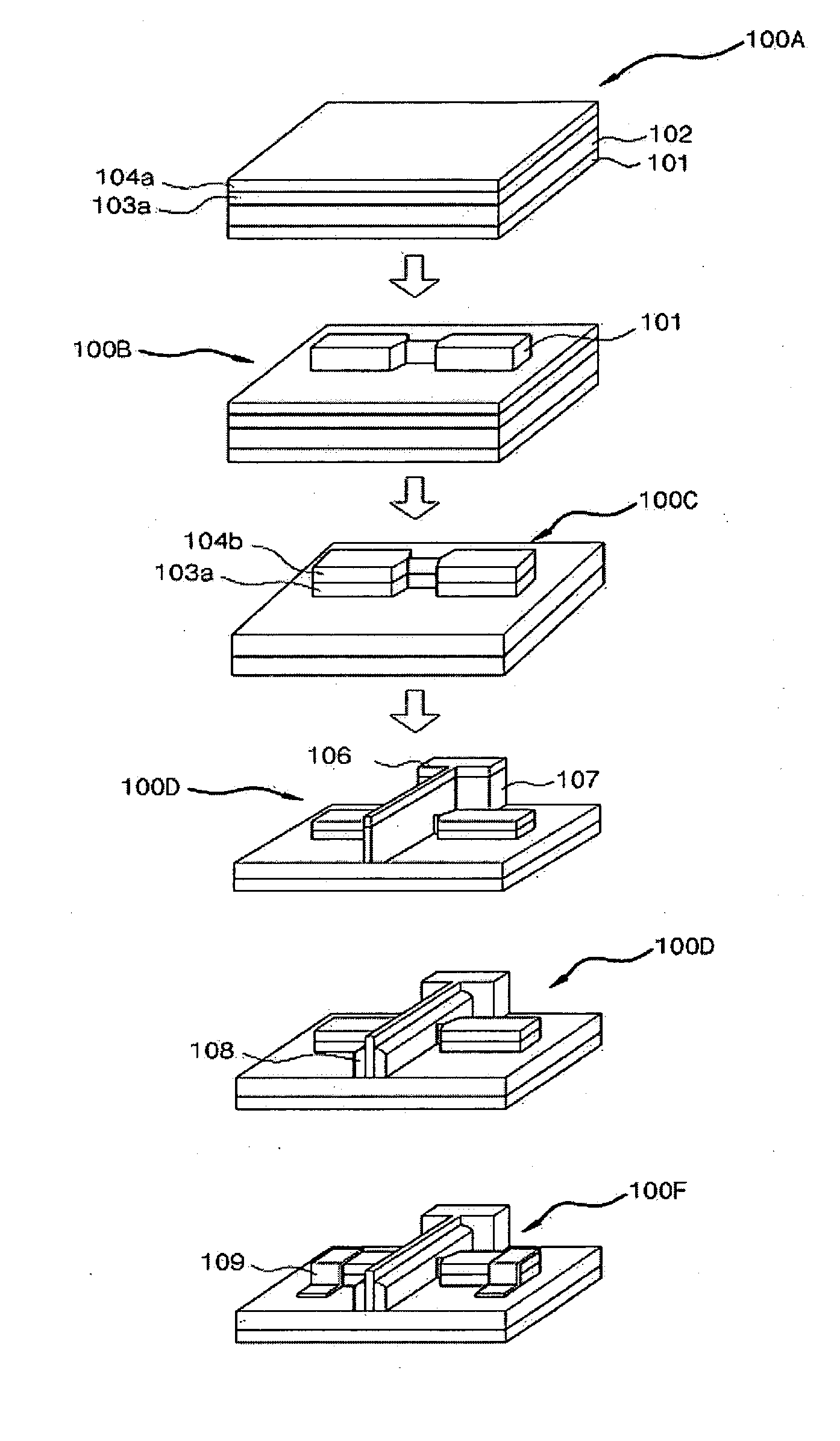
[0058]FIG. 4a is a process perspective view sequentially showing a method for manufacturing a field effect transistor comprising a channel consisting of silicon fins and a silicon body.

[0059] First, an SOI substrate comprising a silicon substrate 401, a buried oxide film 402 and a silicon thin film 403 formed on the buried insulation film 402 is provided. On the silicon thin film 403, a hard mask 404 is formed which is made of a material which will not be etched in subsequent anisotropic or isotropic etching of the silicon thin film (400A).

[0060] In this step, the hard mask 404 may also be formed on a silicon bulk substrate instead of the SOI substrate comprising the silicon substrate 401, the burred oxide film 402 and the silicon thin film 403.

[0061] Then, the silicon thin film 403 is anisotropically etched using the mask pattern 404 as a mask to form a silicon fins 403 where a channel is to be formed, and a silicon pattern 403a where a source / drain region is to be formed. Also,...

embodiment 2

[0072] Embodiment 2 of the present invention is the same as Embodiment 1 except that, after conducting the step (400C) of etching the silicon body using the active mask 405 so as to isolate the source / drain region and the device from each other, the step (400B) of forming the silicon fins using the hard mask 400 is conducted. Accordingly, a drawing showing the second embodiment will be omitted herein.

[0073]FIG. 4b is an a-a′ cross-sectional view of the device manufactured by the method shown in FIG. 4a.

[0074] As can be seen in FIG. 4b, the silicon fins and the silicon body serve as a channel, the orientation of the silicon fins is (110), and the orientation of the silicon body is (100).

[0075] In the case of NMOS according to one embodiment of the present invention, a reduction in electric current by the mobility of electrons in the silicon fins having an orientation of (110) is compensated not only by the effect of an increase in the device channel width in the silicon body but a...

embodiment 3

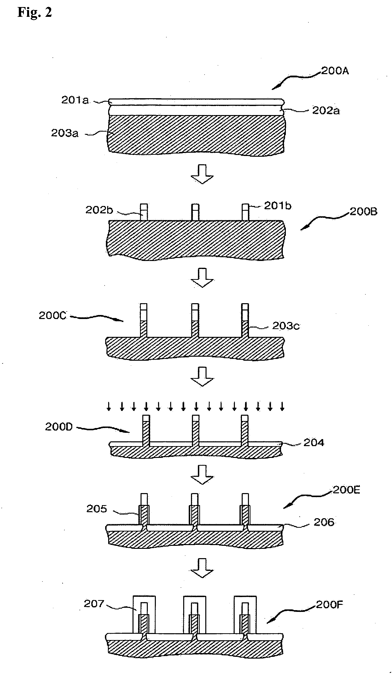
[0077]FIG. 5 is a process cross-sectional view sequentially showing a method for manufacturing a field effect transistor having a channel consisting of silicon fins and a silicon body, according to Embodiment 3 of the present invention.

[0078] First, an SOI substrate comprising a silicon substrate 501, a buried oxide film 502 and a silicon thin film 503 on the buried oxide film 502 is provided (500A).

[0079] In this step, a silicon bulk substrate may also be used instead of the SOI substrate comprising the silicon substrate 501, the buried oxide film 502 and the silicon thin film 503.

[0080] Then, an oxide film 504 is formed on the silicon thin film 503 and etched and patterned using a mask so as to form portions where silicon fins are to be formed (500B).

[0081] In this step, other materials than the oxide film may also be deposited or grown on the silicon thin film 503 and then etched using a mask.

[0082] Next, selective epitaxial growth of silicon is used to form silicon fins 503...


PUM

PropertyMeasurementUnit
channel lengthaaaaaaaaaa
thicknessaaaaaaaaaa
anisotropicaaaaaaaaaa

Abstract

Discloses are a method for manufacturing a field effect transistor comprising a channel consisting of silicon fins and a silicon body, in which the silicon fins have an orientation different from the silicon body, as well as a transistor structure manufactured thereby. The method comprises the steps of: (a) forming a hard mask pattern on a substrate comprising a silicon thin film; (b) anisotropically etching the silicon thin film to a predetermined thickness using the hard mask pattern as a mask so as not only to form silicon fins where a channel is to be formed and a silicon pattern where a source/drain region is to be formed, but also to form a silicon body that connects the silicon fins to each other to form a channel; (c) partially etching the silicon thin film using an active mask so as to isolate the source/drain region and the device from each other; and (d) growing a gate dielectric film around the silicon channel and sequentially depositing a gate material and a gate mask on the resulting structure, followed by forming a gate region.

Description

BACKGROUND OF THE INVENTION [0001] 1. Field of the Invention [0002] The present invention relates to a method for manufacturing a field effect transistor and a transistor structure manufactured by the method. More particularly, the present invention relates to a method for manufacturing a field effect transistor comprising a channel consisting of silicon fins and a silicon body having an orientation different from the silicon fins, as well as a field effect transistor manufactured by the method. [0003] 2. Background of the Related Art [0004] Currently, in an attempt to reduce the price of semiconductor devices and to improve the device performance, the size of semiconductor devices has continued to decrease according to the Moore's law, thus enabling the high integration of semiconductor IC chips. [0005] However, as the channel length of semiconductor devices decreases to less than 100 nm, the potential of a channel in the prior field effect transistors is controlled not only by a g...

Claims


Application Information

Patent Timeline
Patent Type & Authority Applications(United States)
IPC IPC(8): H01L21/84
CPCH01L29/66795H01L29/7842H01L29/7853H01L29/7854
Inventor CHOI, YANG-KYULEE, HYUNJIN
Owner KOREA ADVANCED INST OF SCI & TECH
Why Eureka
Try Eureka