Method and apparatus of reviewing defects on a semiconductor device

a semiconductor device and defect classification technology, applied in material analysis using wave/particle radiation, instruments, nuclear engineering, etc., can solve the problems of difficult reliability of on-film/under-film defect classification, and achieve the effect of high versatility

Active Publication Date: 2007-06-28
HITACHI HIGH-TECH CORP
View PDF3 Cites 19 Cited by
  • Summary
  • Abstract
  • Description
  • Claims
  • Application Information

AI Technical Summary

Benefits of technology

[0006] An embodiment of the invention relates to a method of the on-film/under-film defect classification being robust to the following variation factors, and provides a met

Problems solved by technology

However, reliable on-film/under-film defect classification h

Method used


Image

  • Method and apparatus of reviewing defects on a semiconductor device
  • Method and apparatus of reviewing defects on a semiconductor device
  • Method and apparatus of reviewing defects on a semiconductor device

Examples


Embodiment Construction

[0056] An embodiment of the invention will be described using FIGS. 1 to 14. As an embodiment, while a defect type in on-film / under-film defect classification is described using the particle defect as an example in the following description, an embodiment of the invention can similarly use the pattern defect or the like as the defect type.

[0057] 1. Apparatus Configuration

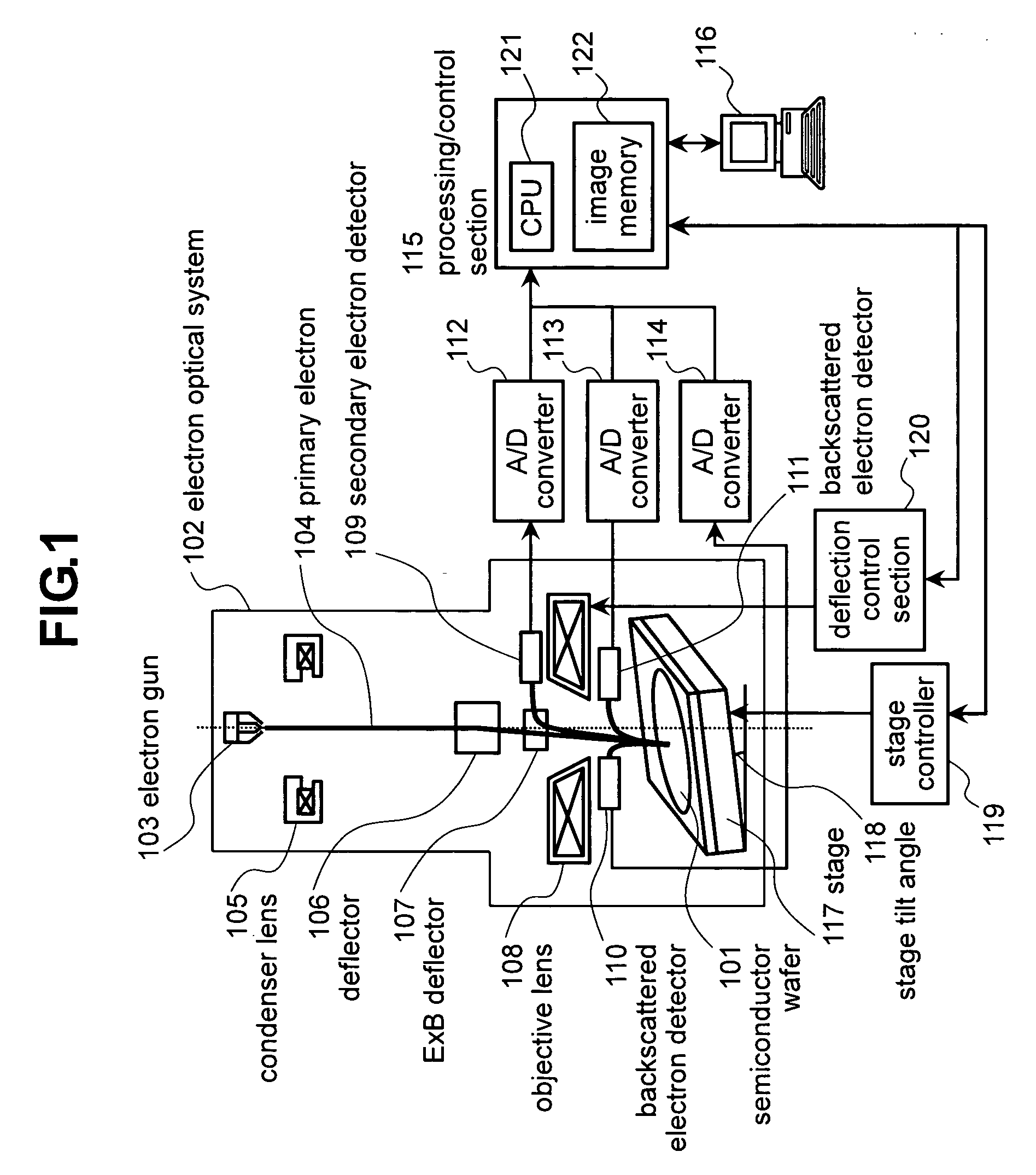
[0058]FIG. 1 shows a block of an outline of a configuration of review SEM apparatus having a scanning electron microscope (SEM) for acquiring a secondary electron image (SE image) or a backscattered electron image (BSE image) of a sample. The SE image and the BSE image are collectively called SEM image. Moreover, images acquired herein include part or all of top down images as images of a measurement object observed in a vertical direction, or tilt images as images of the object observed in a direction of any optional inclination angle.

[0059] A reference 103 indicates an electron gun for generating an electron be...


PUM


Abstract

To realize reliable on-film/under-film defect classification (classification into 3 classes of on-film, under-film, and determination-disabled) with determination propriety determination, an on-film/under-film defect classification method and a method of narrowing a range of defect generation timing are given, the methods being robust to 4 variation factors, wherein an edge of a boundary line between a line pattern region and a base region is focused, and whether the edge is preserved between defect and reference images in a defective region is determined, thereby an on-film or under-film defect can be identified. Furthermore, a range of the defect generation timing can be narrowed based on an identification result of the on-film or under-film defect, and information of a defect classification class (defect type) such as particle defect or pattern defect as necessary.

Description

BACKGROUND OF THE INVENTION [0001] The present invention relates to a method and apparatus of reviewing defects, which acquire a detailed image of defects on a semiconductor wafer inspected by another inspection apparatus and reviews the defects, and particularly relates to a method and apparatus of reviewing defects, which perform automatic defect classification (ADC) for identifying an adhesion process of defects in a semiconductor manufacturing process from images of the defects on a semiconductor wafer observed by a scanning electron microscope (SEM). DESCRIPTION OF RELATED ART [0002] The semiconductor device is manufactured by repeatedly performing a plurality of manufacturing steps to a wafer to be a substrate, such as steps of deposition, resist coating, exposure, development, and etching, and after treatment in each of predetermined steps among the plurality of treatment steps, identification of positions or inspection of size of defects is performed using optical or SEM-typ...

Claims


Application Information

Patent Timeline
IPC IPC(8): G21K7/00
CPCH01J37/222H01J37/265H01J37/28H01J2237/24578H01J2237/2487H01J2237/2817
Inventor MIYAMOTO, ATSUSHIHONDA, TOSHIFUMI
Owner HITACHI HIGH-TECH CORP
Why Eureka
Try Eureka