III-Nitride Light Emitting Device with Double Heterostructure Light Emitting Region

a light emitting device and heterostructure technology, applied in the direction of semiconductor devices, basic electric elements, electrical appliances, etc., can solve the problem of devices suffering from decreasing efficiency

Active Publication Date: 2007-06-28
LUMILEDS
View PDF11 Cites 8 Cited by
  • Summary
  • Abstract
  • Description
  • Claims
  • Application Information

AI Technical Summary

Problems solved by technology

At higher drive currents desirable for lighting, these devices suffer decreasing efficiency with increasing current density.

Method used


Image

  • III-Nitride Light Emitting Device with Double Heterostructure Light Emitting Region
  • III-Nitride Light Emitting Device with Double Heterostructure Light Emitting Region
  • III-Nitride Light Emitting Device with Double Heterostructure Light Emitting Region

Examples


Embodiment Construction

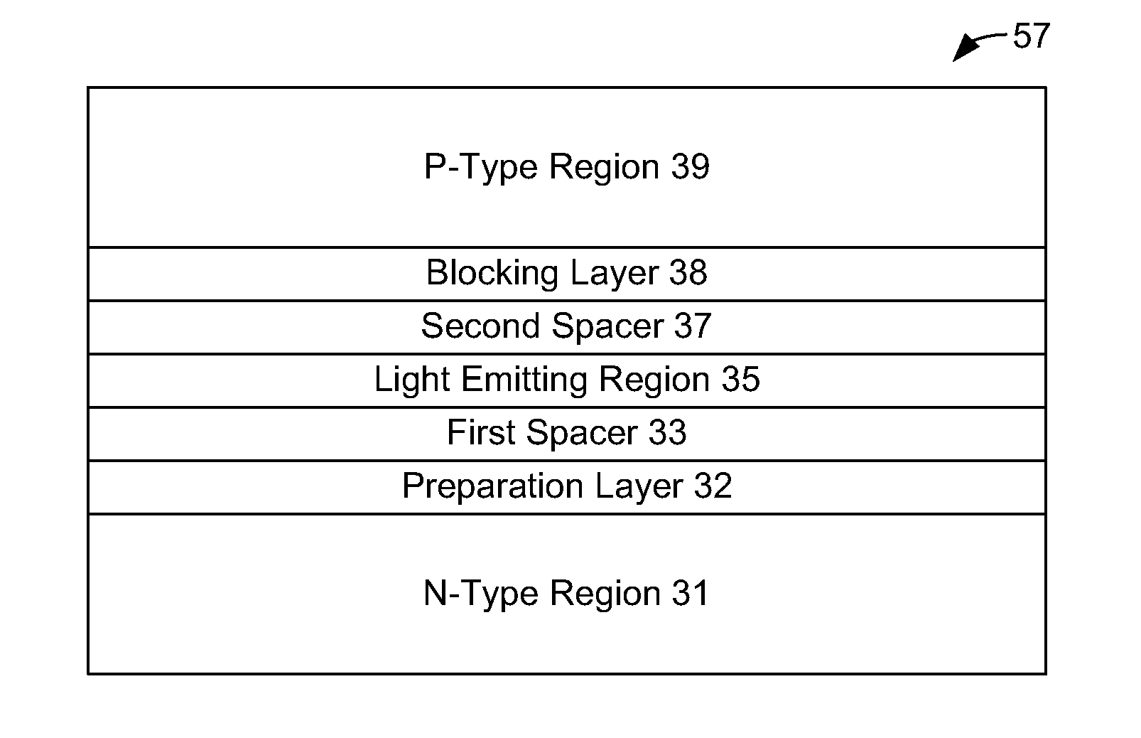
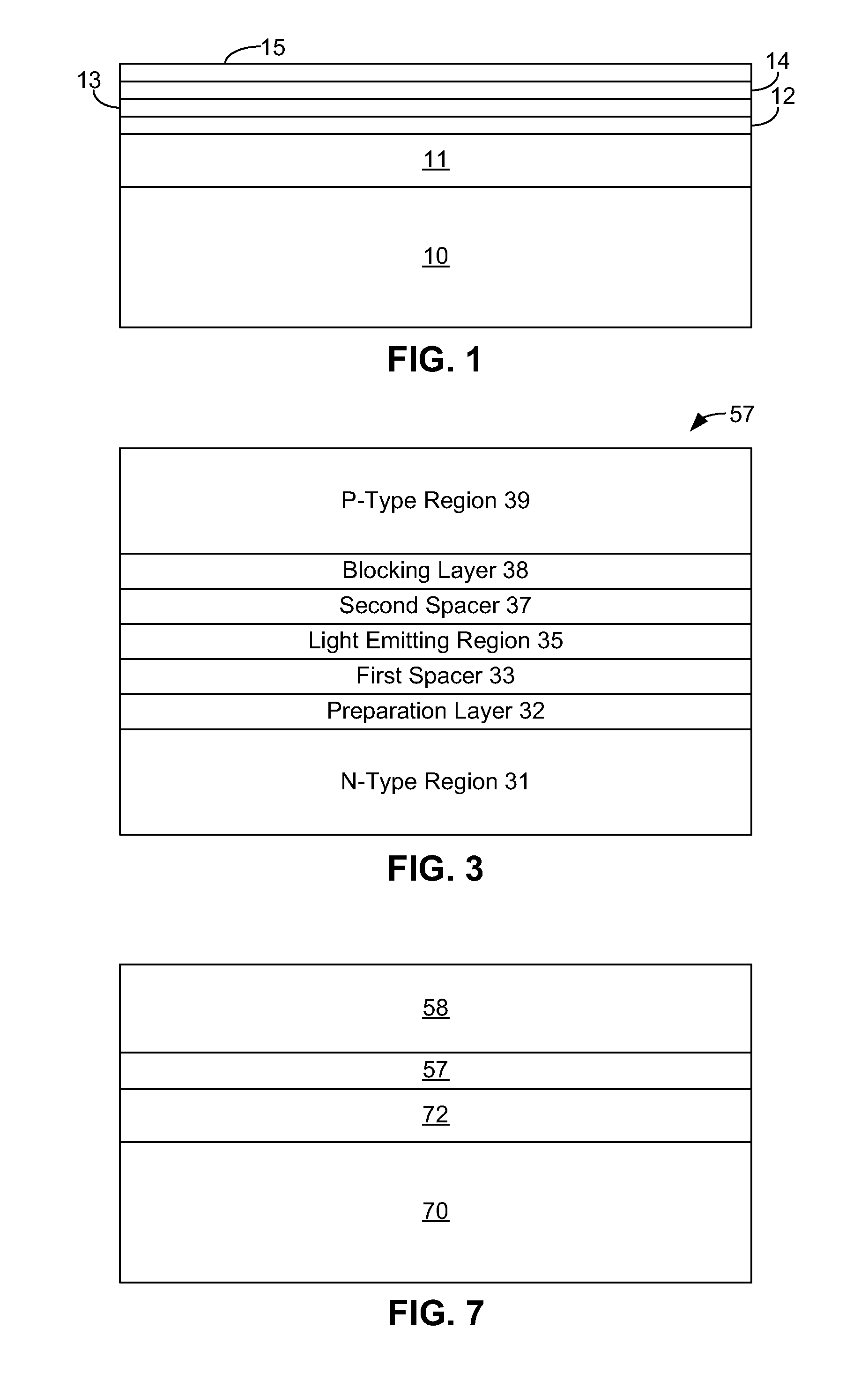
[0021]FIG. 1 illustrates a common III-nitride light emitting device. An n-type region 11 is grown over a sapphire substrate 10. An active region 12, including multiple thin quantum well layers separated by barrier layers, is grown over n-type region 11, followed by a GaN spacer layer 13, a p-type AlGaN layer 14, and a p-type contact layer 15.

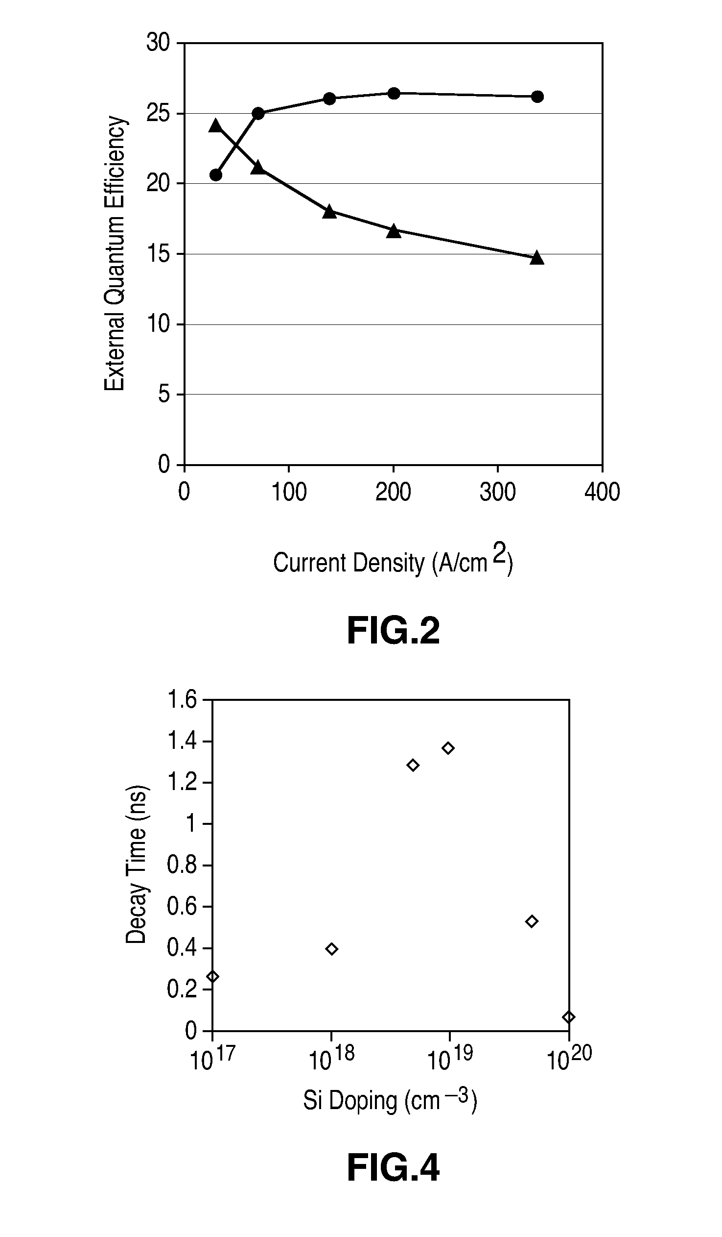
[0022]FIG. 2 illustrates the external quantum efficiency of a device such as the device of FIG. 1 (triangles on FIG. 2) and a device according to an embodiment of the present invention (circles on FIG. 2). The external quantum efficiency is the internal quantum efficiency, defined as the flux of photons produced divided by the flux of carriers supplied, multiplied by the extraction efficiency. For a given lamp design, the extraction efficiency is constant, thus the extraction efficiency is the same for both devices shown in FIG. 2. As the current density applied to the device of FIG. 1 increases, the external quantum efficiency of the device in...


PUM


Abstract

In a device, a III-nitride light emitting layer is disposed between an n-type region and a p-type region. A first spacer layer, which is disposed between the n-type region and the light emitting layer, is doped to a dopant concentration between 6×1018 cm3 and 5×1019 cm−3. A second spacer layer, which is disposed between the p-type region and the light emitting layer, is not intentionally doped or doped to a dopant concentration less than 6×1018 cm−3.

Description

CROSS REFERENCE TO RELATED APPLICATIONS [0001] This application is a continuation of U.S. patent application Ser. No. 11 / 211,921, filed Aug. 24, 2005.BACKGROUND [0002] 1. Field of Invention [0003] This invention relates to the light emitting region of a semiconductor light emitting device. [0004] 2. Description of Related Art [0005] Semiconductor light-emitting devices including light emitting diodes (LEDs), resonant cavity light emitting diodes (RCLEDs), vertical cavity laser diodes (VCSELs), and edge emitting lasers are among the most efficient light sources currently available. Materials systems currently of interest in the manufacture of high-brightness light emitting devices capable of operation across the visible spectrum include Group III-V semiconductors, particularly binary, ternary, and quaternary alloys of gallium, aluminum, indium, and nitrogen, also referred to as III-nitride materials. Typically, III-nitride light emitting devices are fabricated by epitaxially growing ...

Claims


Application Information

Patent Timeline
Patent Type & Authority Applications(United States)
IPC IPC(8): H01L33/00H01L33/06H01L33/32
CPCH01L33/06H01L33/32H01L33/025H01L33/325H01L33/02
Inventor GARDNER, NATHAN F.CHEN, GANGYIGOETZ, WERNER K.KRAMES, MICHAEL R.MUELLER, GERD O.SHEN, YU-CHENWATANABE, SATOSHI
Owner LUMILEDS
Why Eureka
Try Eureka