Sense amplifier for semiconductor memory device
a technology of memory device and sense amplifier, which is applied in the direction of semiconductor devices, digital storage, instruments, etc., can solve the problems of significant change of operation speed, heavy load capacity of local io line, and difficulty in high-speed operation
- Summary
- Abstract
- Description
- Claims
- Application Information
AI Technical Summary
Problems solved by technology
Method used
Image
Examples
first embodiment
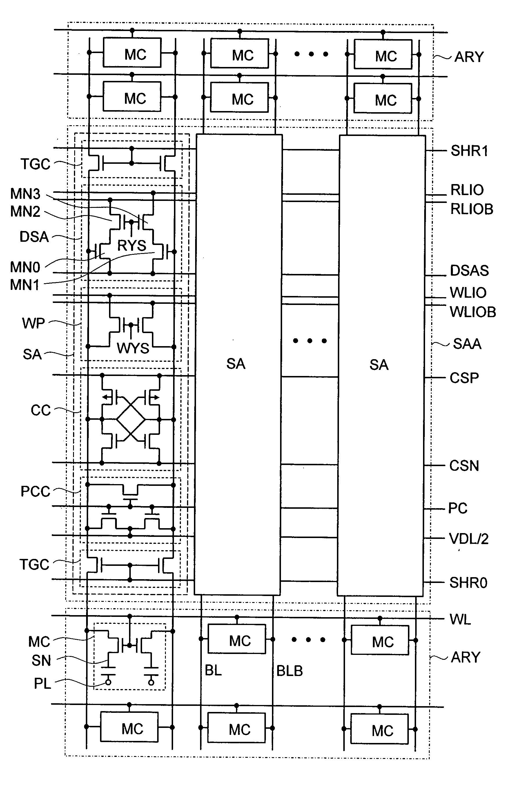
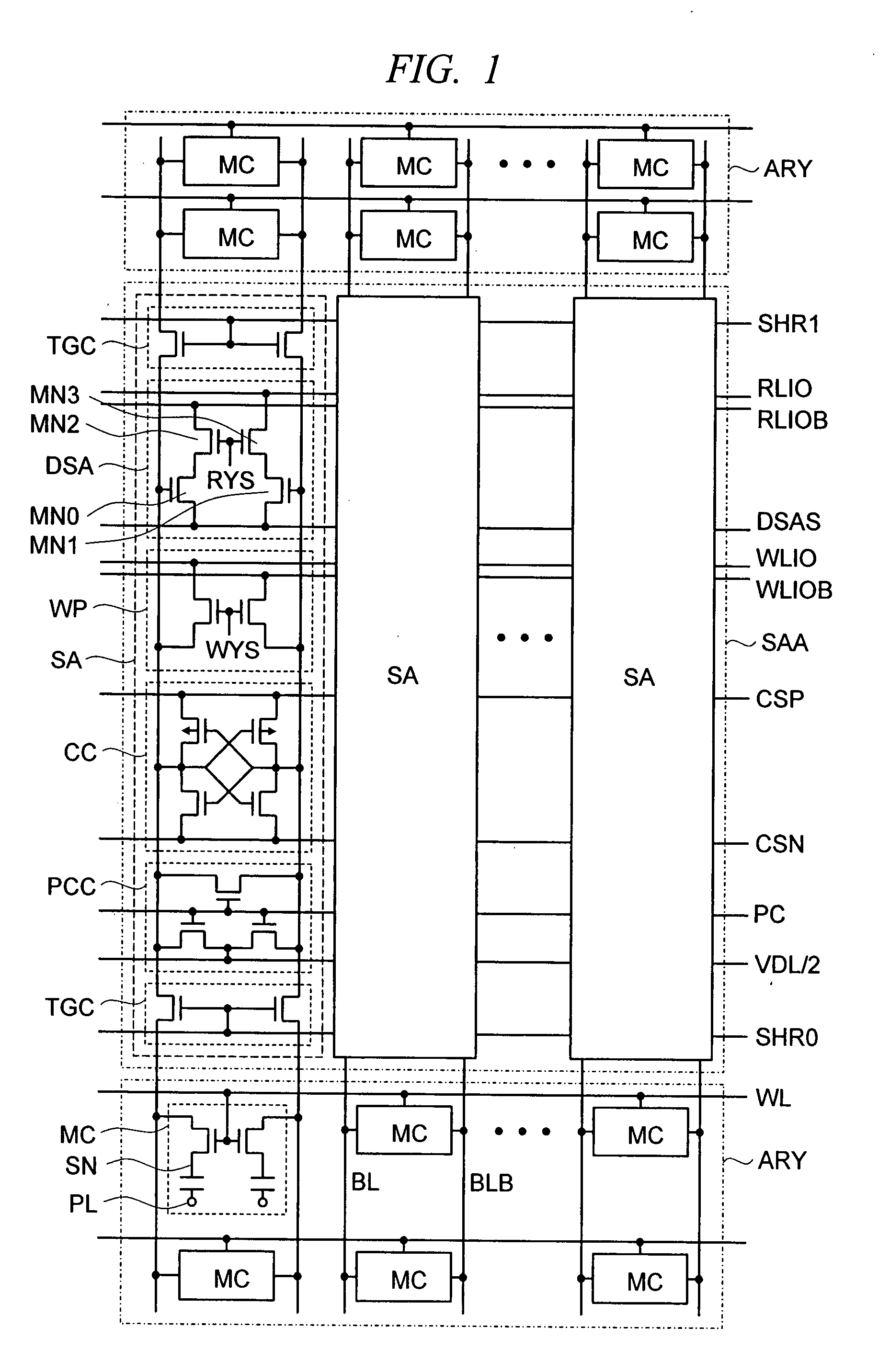
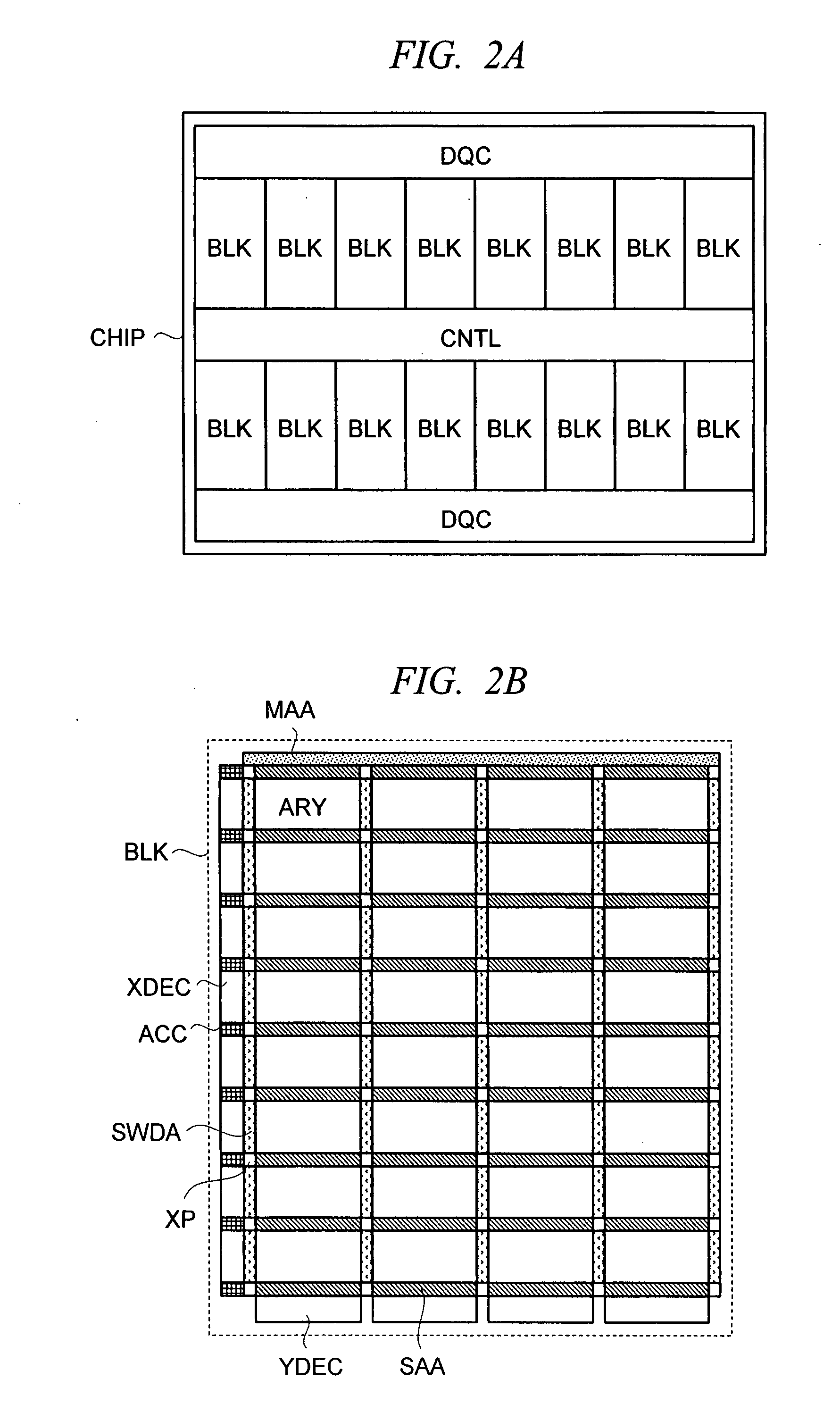
[0034]FIG. 1 shows memory arrays ARY and sense amplifiers SA according to the present invention. To describe a function of the sense amplifier, a chip structure of a semiconductor memory device according to the present invention is shown in FIG. 2A. The entire chip CHIP is broadly divided into a control circuit CNTL, input / output circuits DQC, and memory blocks BLK. A clock, an address, and a control signal are supplied to the control circuit from the outside of the chip to determine an operation mode of the chip and pre-decode the address. The input / output circuit includes an input / output buffer, so that write date is inputted from the outside of the chip and read data is outputted to the outside of the chip.
[0035] A structure of the memory block BLK is shown in FIG. 2B. On the memory block, memory arrays ARY are disposed on a plurality of arrays, and are each surrounded by sense amplifier columns SAA, sub-word driver columns SWDA, and cross areas XP. Also, column decoders YDEC an...
second embodiment
[0062]FIG. 20 shows a connection method of a second local IO according to the present invention. By using this connection method, when the direct sense amplifier DSA and the write circuit WP in one sense amplifier SA are connected to different local IO lines, data of two bits can be read from one sense amplifier column during the reading and writing by using two set of LIO line pairs.
[0063] For this reason, the sense amplifiers are divided into a group “a” and a group “b” at a center of one sense amplifier column SAA. In the group “a”, the write circuit WP is connected to one local IO line pair LIO0 / LIO0B, and the direct sense amplifier DSA is connected to the other local IO line pair LIO1 / LIOB1. Conversely in the group “b”, the write circuit WP is connected to the local IO line pair LIO1 / LIO1B, and the direct sense amplifier DSA is connected to the other local IO line pair LIO1 / LIOB1.
[0064] During the reading, when one RYS is activated from each of the groups “a” and “b”, the dat...
third embodiment
[0065]FIG. 21 shows a second data-path structure according to the present invention. In the data path according to the present invention, since an offset-compensated sub amplifier is disposed in a connection portion of a local IO line and a main IO line, the offset of the direct sense amplifier can be compensated without providing an offset compensation for the direct sense amplifier itself. A memory array ARY and a sense amplifier SA therein are identical to those shown in FIG. 1, and therefore only respective portions thereof are illustrated. What is different in the present invention is that a sub amplifier BA is provided in the cross area XP. The other circuits except the cross area are the same to those of FIG. 5 and therefore are omitted in FIG. 21.
[0066] An operation of the data path according to the present invention will be described by using operation waveforms of FIG. 22. When the read command RD is inputted, the pre-charge signal PC is deactivated at the VSS. Almost at ...
PUM
 Abstract
Description
Claims
Application Information


