Method of fabricating complementary metal oxide silicon image sensor

a technology of complementary metal oxide silicon and image sensor, which is applied in the direction of semiconductor devices, radio frequency controlled devices, electrical apparatus, etc., can solve the problems of deteriorating process effectiveness and pop-up defect peeled from the wafer edge, and achieves improved low illumination characteristics, improved sensitivity, and increased hydrogen anneal

Active Publication Date: 2007-06-28
DONGBU HITEK CO LTD
View PDF12 Cites 10 Cited by
  • Summary
  • Abstract
  • Description
  • Claims
  • Application Information

AI Technical Summary

Benefits of technology

[0014] An object of the present invention is to provide a method of fabricating a CMOS image sensor that drastically enhances sensitivity by removing a passivation nitride in a pixel region of a CMOS image sensor, improving a...

Problems solved by technology

Since a passivation nitride is applied thickly, it has a tendency to block hydrogen ions, thereby deteriorating process effectivenes...

Method used


Image

  • Method of fabricating complementary metal oxide silicon image sensor
  • Method of fabricating complementary metal oxide silicon image sensor
  • Method of fabricating complementary metal oxide silicon image sensor

Examples


Embodiment Construction

[0022] Reference will now be made in detail to the preferred embodiments of the present invention, examples of which are illustrated in the accompanying drawings. Wherever possible, the same reference numbers will be used throughout the drawings to refer to the same or like parts.

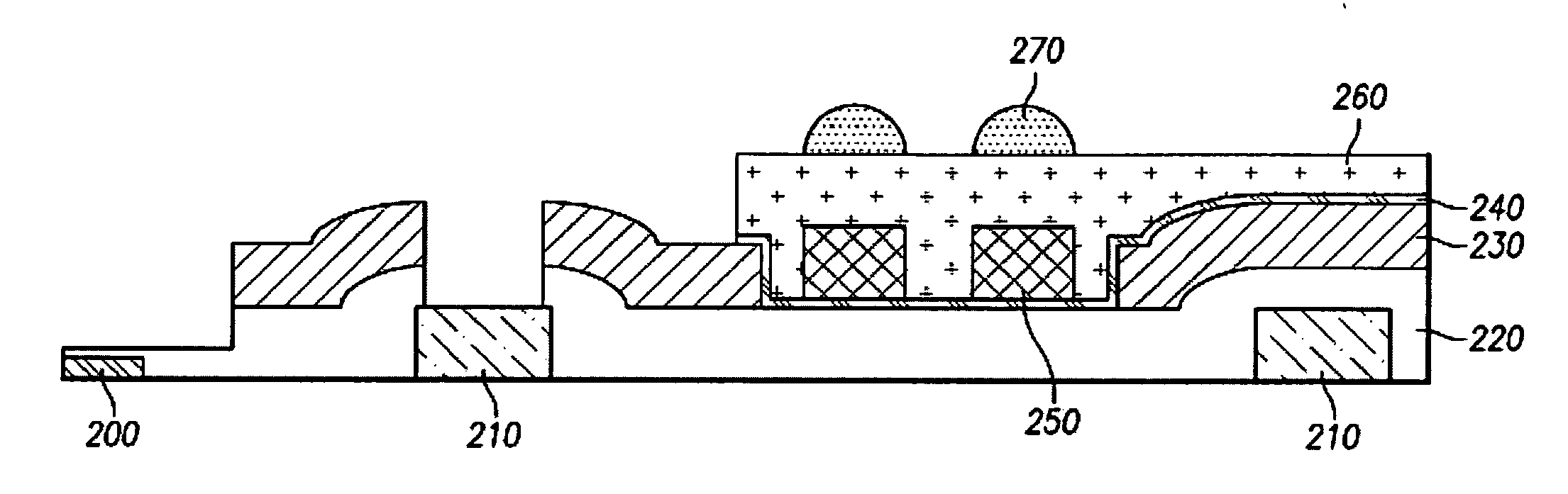
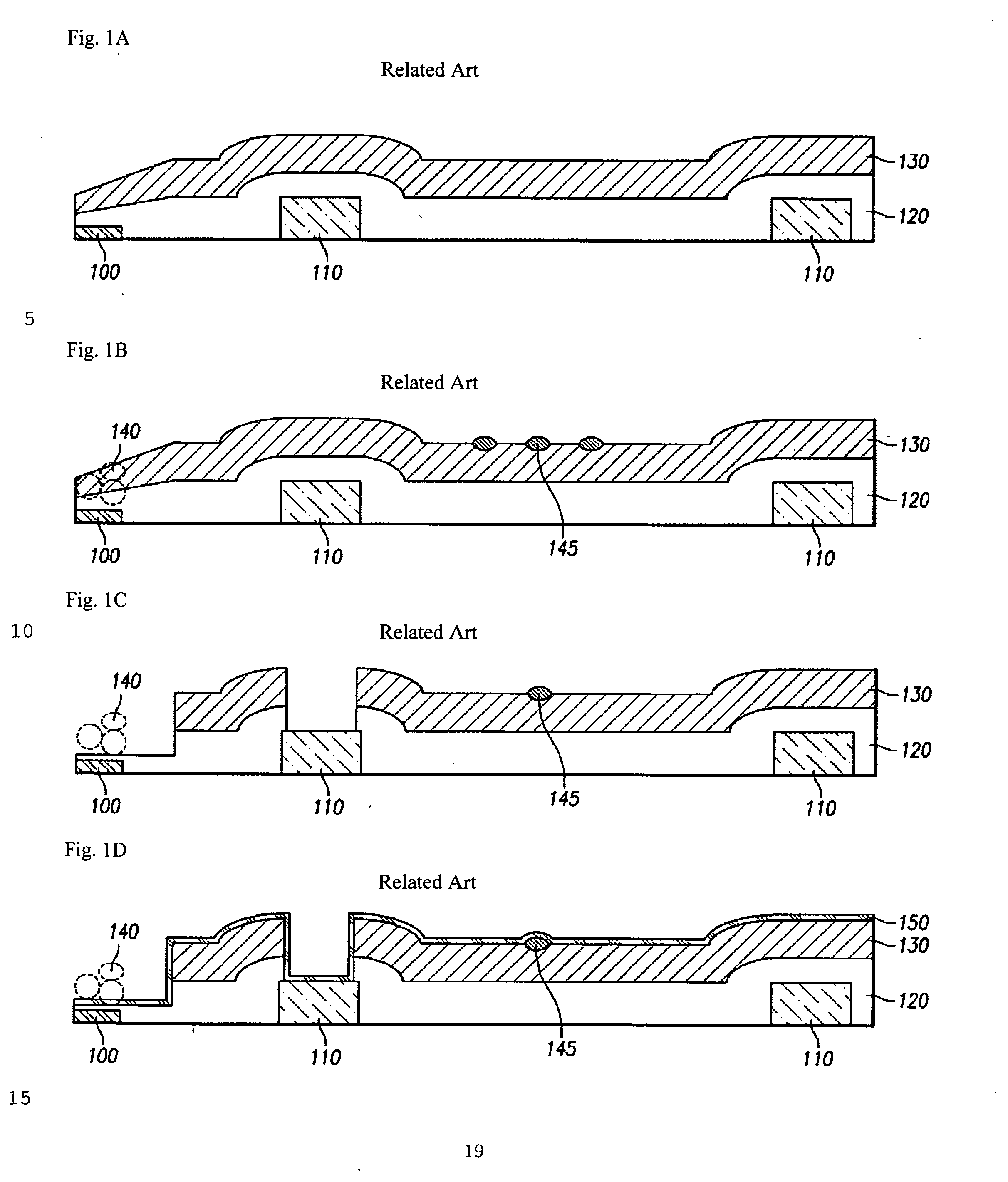
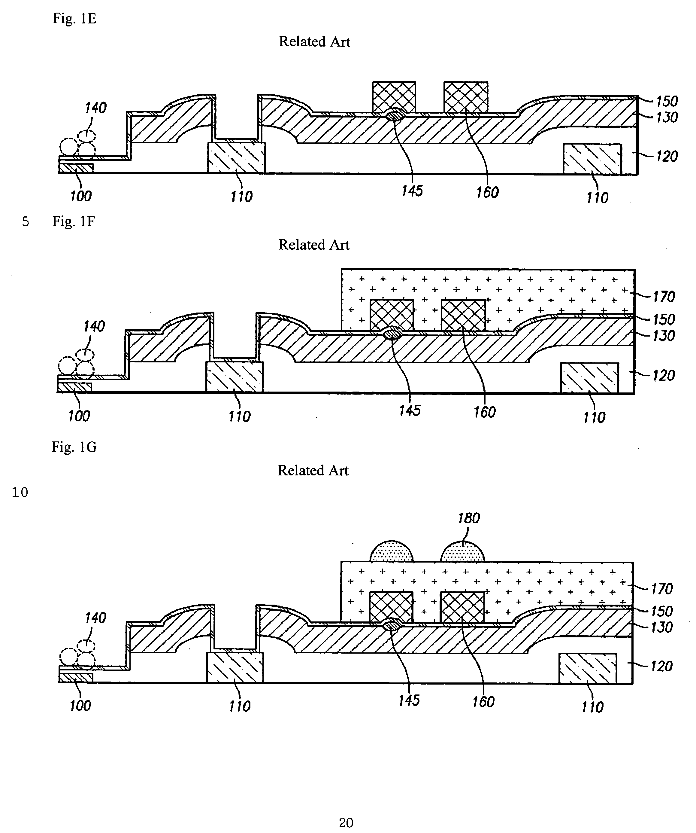
[0023]FIGS. 2A through 2I are sectional views illustrating a method of fabricating a CMOS image sensor according to an embodiment of the present invention. FIGS. 2A through 2D are sectional views of processes after forming a pad 210.

[0024] Referring to FIG. 2A, after forming a pad 210, a passivation oxide 220 and a passivation nitride 230 are sequentially-applied. After applying the passivation oxide 220, a chemical mechanical planarization process is performed and then the passivation nitride 230 is applied. On the other hand, unlike an actual main chip region inside a wafer, an irregular wafer edge remaining layer 200 remains in an edge region of the wafer due to a wafer edge going through various photo...


PUM


Abstract

Provided is a method of fabricating a complementary metal oxide silicon image sensor. The method includes: applying a passivation oxide and a passivation nitride after forming a pad; selectively removing the passivation nitride in a pad region and a pixel region by a photolithography process, and performing a first cleaning process; performing a hydrogen anneal process; opening the pad by removing the passivation oxide in the pad region and performing a second cleaning process; applying a pad protective layer; performing a color filter array process, a planarization process, and a microlens process after the applying of the pad protective layer; and removing the pad protective layer in the pad region.

Description

BACKGROUND OF THE INVENTION [0001] 1. Field of the Invention [0002] The present invention relates to a method of fabricating a semiconductor device, and more particularly, to a method of fabricating a complementary metal oxide silicon (CMOS) image sensor. The present invention relates to especially to a process after forming a pad from a metal line layer. [0003] 2. Description of the Related Art [0004] Characteristics of a CMOS image sensor depend on sensitivity of a photo diode receiving external light particles. This sensitivity is mainly determined by a distance between a microlens and a photo diode, and also a thin film characteristic. Unlike a metal layer that completely reflects all light, a passivation nitride of a related art pixel block generally screens and reflects a relatively large portion of light compared to a passivation oxide. Accordingly, the sensitivity of a CMOS image sensor deteriorates. [0005] On the other hand, a hydrogen anneal process, e.g., a sintering proc...

Claims


Application Information

Patent Timeline
IPC IPC(8): H01L21/00
CPCH01L27/14627H01L27/14683H01L27/14685H01L27/146
Inventor KIM, JIN HAN
Owner DONGBU HITEK CO LTD
Why Eureka
Try Eureka