
Vertical cavity surface emitting laser

a laser and vertical cavity technology, applied in the direction of semiconductor lasers, laser details, electrical apparatus, etc., can solve the problems of difficult to manufacture vcsel devices, and achieve the effects of reducing the resistance of the device, increasing the thickness of the current confinement layer, and reducing electrical power consumption

Active Publication Date: 2007-07-05
SONY CORP
View PDF5 Cites 14 Cited by
  • Summary
  • Abstract
  • Description
  • Claims
  • Application Information

AI Technical Summary

Benefits of technology

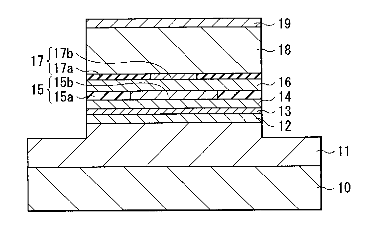
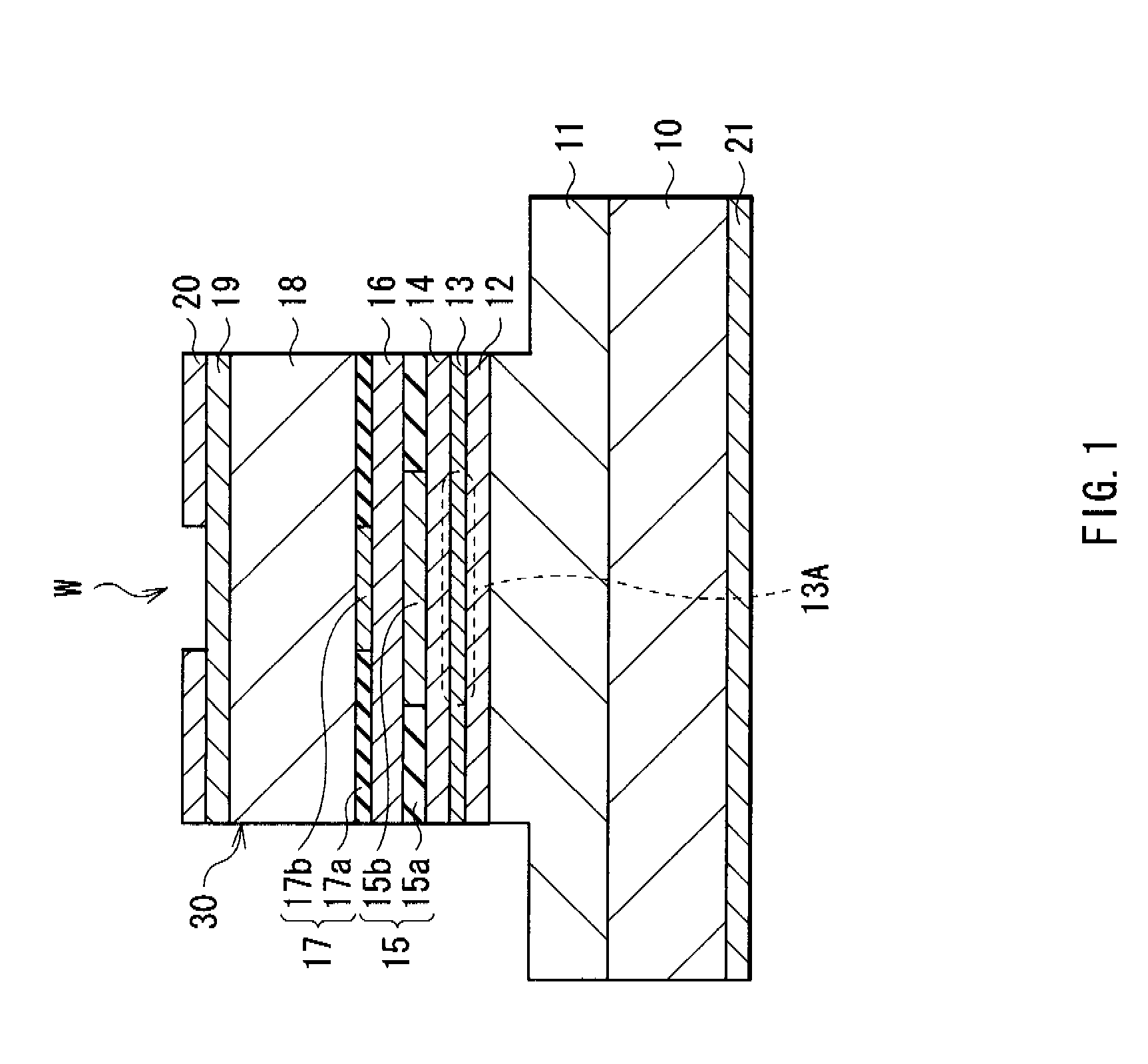
[0013] In the VCSEL of the embodiment of the invention, the second current confinement layer with the thickness thinner than that of the first current confinement layer and with the diameter of the second current injection region smaller than that of the first current injection region is provided at the node of the standing wave. Therefore, in the second current confinement layer, a current is confined with giving no loss to light. Thereby, the diameter of the second current injection region can be decreased to the degree that the current density becomes almost uniform over the whole area of the second current injection region. The second current confinement layer is provided in a position farther from the active layer than the first current confinement layer. Therefore, when the diameter of the second current injection region is set to the size with which the current density becomes almost uniform over the whole area of the second current injection region, the current confined by the second current confinement layer is not concentrated on the outer edge of the first current injection region of the first current confinement layer, and the current is concentrated on the central portion of the first current injection region. In the result, it becomes possible to intensively inject the current into the central portion of the region corresponding to the first current injection region in the active layer (central portion of the light emitting region). Meanwhile, the first current confinement layer with the thickness thicker than that of the second current confinement layer and with the diameter of the first current injection region larger than that of the second current injection region is provided at the antinode of the standing wave. Therefore, in the first current confinement layer, a loss is given to light in the transverse mode with the order having a large gain in the portion corresponding to the outer edge of the first current injection region (outer edge of the light emitting region), and a loss is hardly given to light in the transverse mode with the order having a large gain in the portion corresponding to the central portion of the first current injection region (central portion of the light emitting region).
[0014] According to the VCSEL of the embodiment of the invention, the first current confinement layer having the first current injection region with the large diameter and the second current confinement layer having the second current injection region with the small diameter are provided in this order from the active layer side. Therefore, a current can be intensively injected into the central portion of the light emitting region of the active layer. Thereby, compared to a case that the current density is concentrated on the outer edge of the light emitting region, only oscillation in the high-order transverse mode having a large gain in the outer edge in the light emitting region can be selectively suppressed. Since the thin second current confinement layer is provided at the node of the standing wave, a loss is hardly given to light regardless of the diameter size of the second current injection region, and oscillation in the basic lateral mode having a large gain in the central portion of the light emitting region is hardly blocked.
[0015] Further, as described above, the second current confinement layer has a function to confine a current. Therefore, it is possible to relatively freely set the diameter size of the first current injection region of the first current confinement layer provided at the antinode of the standing wave. When the diameter size of the first current injection region is appropriately adjusted, it is possible that a loss is hardly given to the light in the basic lateral mode having a large gain in the central portion of the light emitting region, and a loss is selectively given to only the light in the high-order lateral mode having a large gain in the outer edge of the light emitting region.
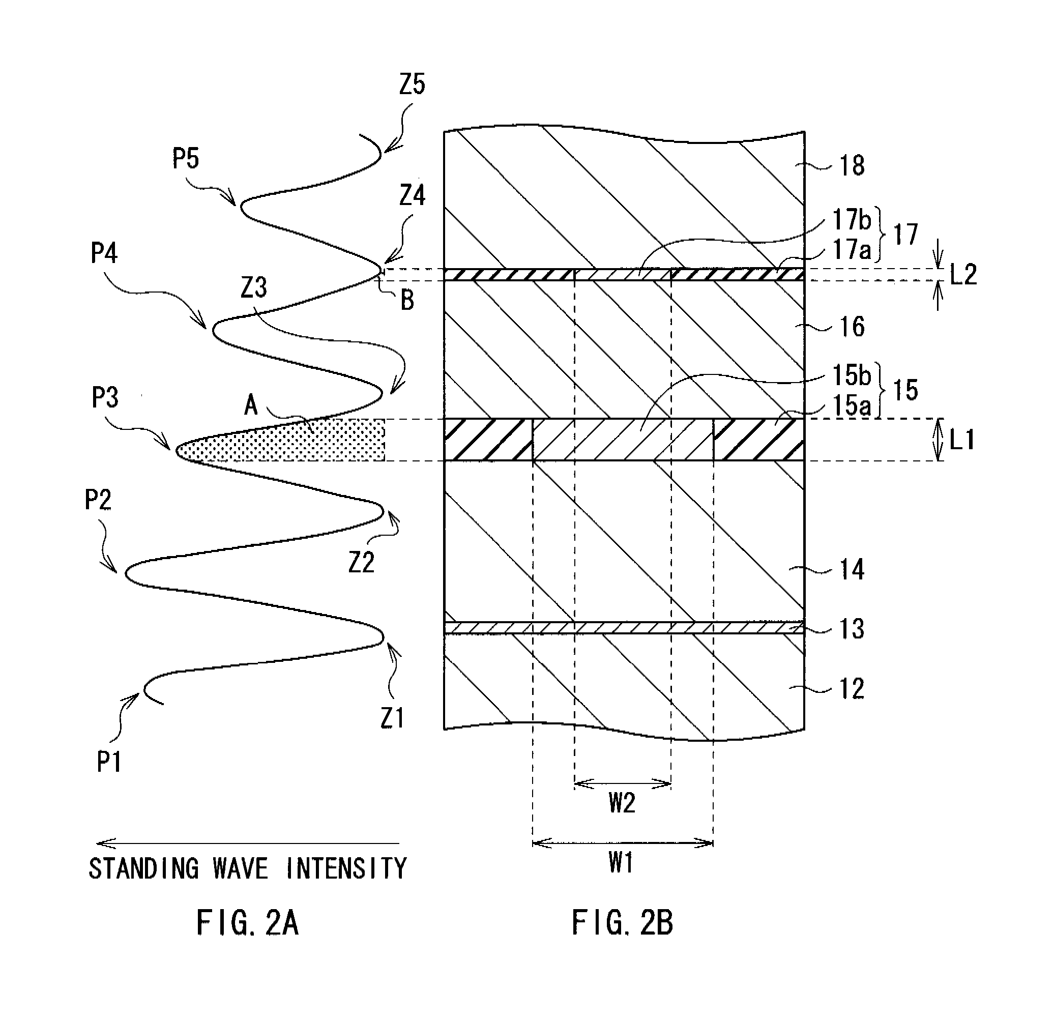
[0017] When the first current confinement layer has a thickness so that an integral value (area) of the standing wave intensity in the region corresponding to the first current confinement layer is 0.5 or more and smaller than 1.0 where an integral value (area) of the standing wave intensity in a region between two nodes located on the both sides of the antinode of the standing wave corresponding to the first current confinement layer is 1.0, a loss to the light in the basic lateral mode given from the first current confinement layer can be extremely small. Further, when the second current confinement layer has a thickness so that an integral value (area) the standing wave intensity in a region corresponding to the second current confinement layer is smaller than 0.1 where an integral value (area) of the standing wave intensity in a region between two nodes located on the both sides of the node of the standing wave corresponding to the second current confinement layer is 1.0, a light loss in the second current confinement layer can be extremely small. Thereby, it is possible to further improve the light output in the basic lateral mode while suppressing the oscillation in the high-order lateral mode.

Problems solved by technology

As above, in the existing techniques, it has been difficult to easily manufacture a VCSEL device which can selectively prevent only the high-order transverse mode oscillation.

Method used


Image

  • Vertical cavity surface emitting laser
  • Vertical cavity surface emitting laser
  • Vertical cavity surface emitting laser

Examples


first embodiment

[0028]FIG. 1 shows a cross sectional structure of a VCSEL according to an embodiment of the invention. FIG. 2A shows standing wave intensity in a first current confinement layer 15 and a second current confinement layer 17 of the VCSEL of FIG. 1 and in the vicinity thereof. FIG. 2B shows an enlarged cross section of the first current confinement layer 15 and the second current confinement layer 17 of the VCSEL of FIG. 1 and the vicinity thereof. FIG. 1, FIG. 2A, and FIG. 2B show the views as a model, and thus the dimensions and the shapes thereof are different from actual dimensions and shapes.

[0029] The VCSEL includes a resonator in which an n-type DBR layer 11 (second multilayer reflector), an n-type guide layer 12, an active layer 13, a p-type guide layer 14, the first current confinement layer 15, a spacer layer 16, the second current confinement layer 17, a p-type DBR layer 18 (first multilayer reflector), and a p-type contact layer 19 are layered in this order on one face of ...


PUM


Abstract

A VCSEL which can be easily manufactured and can selectively suppress only high-order transverse mode oscillation is provided. The VCSEL includes a resonator, a first current confinement layer, and a second current confinement layer. The resonator includes an active layer having a light emitting region, and a pair of first multilayer reflector and a second multilayer reflector provided with the active layer in between, and resonate is generated in a given wavelength. The first current confinement layer has a current injection region is a region corresponding to the light emitting region, and is formed at a region including an antinode of a standing wave. The second current confinement layer has a current injection region with a diameter smaller than a diameter of the first current injection region and is formed at a region including a node standing wave.

Description

CROSS REFERENCES TO RELATED APPLICATIONS [0001] The present invention contains subject matter related to Japanese Patent Application JP 2005-364912 filed in the Japanese Patent Office on Dec. 19, 2005, the entire contents of which being incorporated herein by reference. BACKGROUND OF THE INVENTION [0002] 1. Field of the Invention [0003] The present invention relates to a vertical cavity surface emitting laser (VCSEL) which has a laser light emitting region on the top face, particularly to a VCSEL which can be suitably applied to purposes necessitating light output in the low-order transverse mode. [0004] 2. Description of the Related Art [0005] A VCSEL emits light in the direction perpendicular to the substrate unlike the existing edge-emitting laser diodes. In the VCSEL, many devices can be arranged in a state of a two dimensional array on the same substrate. Therefore, the VCSEL has recently attracted attention as a light source for a digital copy machine or a printer. [0006] In t...

Claims


Application Information

Patent Timeline
Patent Type & Authority Applications(United States)
IPC IPC(8): H01S5/00
CPCH01S5/18311H01S2301/166H01S5/18338H01S5/18333H01S5/183H01S5/187
Inventor MAEDA, OSAMUSHIOZAKI, MASAKI
Owner SONY CORP
Features
  • Generate Ideas
  • Intellectual Property
  • Life Sciences
  • Materials
  • Tech Scout
  • Unparalleled Data Quality
  • Higher Quality Content
  • 60% Fewer Hallucinations
Learn More