Corresponding capacitor arrangement and method for making the same

Inactive Publication Date: 2007-07-05
INFINEON TECH AG
View PDF7 Cites 24 Cited by
  • Summary
  • Abstract
  • Description
  • Claims
  • Application Information

AI Technical Summary

Benefits of technology

[0010] Accordingly, in the method according to the invention only a first insulating layer is formed at the surface of a carrier substrate and a first capacitor electrode with a multiplicity of interspaced first interconnects is subsequently produced in the first insulating layer. Afterward, for the purpose of uncovering at least partial regions of the first insulating layer between the multiplicity of first interconnects, a mask layer is formed and the uncovered partial regions of the first insulating layer are thereby removed for the purpose of uncovering the multiplicity of first interconnects, in particular the lateral areas thereof. After the removal of the mask layer, a capacitor dielectric is formed at least at the surface of the uncovered first interconnects and, finally, a second capacitor electrode is formed at the surface of the capacitor dielectric with a multiplicity of interspaced second interconnects lying between the first interconnects. The omission of at leas

Problems solved by technology

What is disadvantageous in this case, on account of the large thicknesses of the interlayer dielectric of approximately 200 to 500 nanometers, is a very high amount of space taken up for realizing sufficiently high capacitances.

Method used


Image

  • Corresponding capacitor arrangement and method for making the same
  • Corresponding capacitor arrangement and method for making the same
  • Corresponding capacitor arrangement and method for making the same

Examples


Embodiment Construction

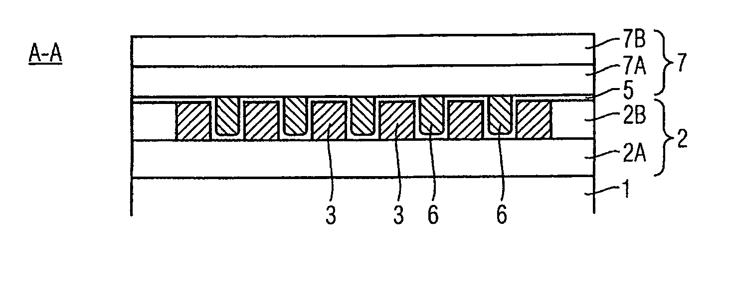
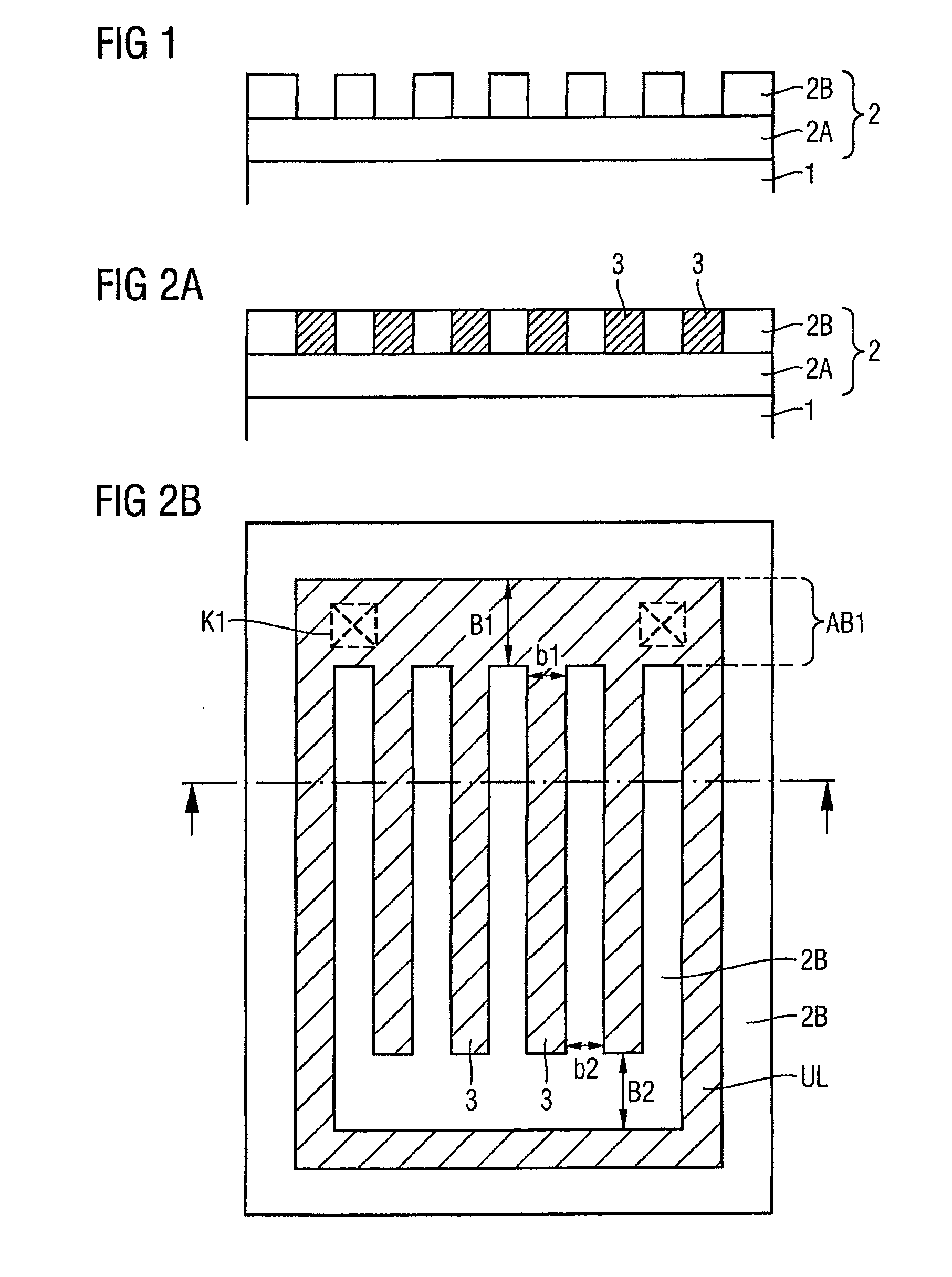
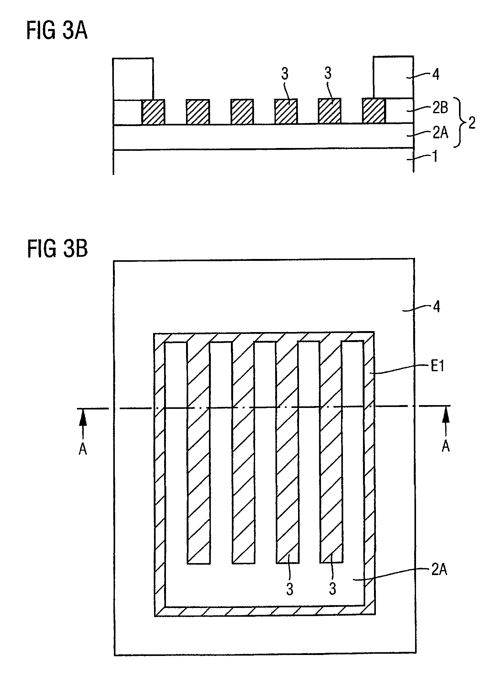
[0019] In accordance with FIG. 1, firstly a first insulating layer 2 is formed over the whole area at the surface of a carrier substrate 1 and a multiplicity of depressions or trenches for a later first capacitor electrode are produced in an upper region of the first insulating layer 2 for example by means of a damascene method.

[0020] In this case, the carrier substrate 1 used is usually a semiconductor wafer which has been partly processed in an FEOL process and in which a multiplicity of semiconductor components such as e.g. transistors, etc. have already been formed. The topmost layer of the carrier substrate 1 may consequently constitute a first metalization level or an interlayer dielectric (ILD) lying thereon. Preferably, the layer levels illustrated in the figures are situated in one of the bottommost metalization levels or the so-called “1× levels”, in which a minimum line width or feature size prevails and maximum capacitances per unit area can thus be realized. On the oth...


PUM


Abstract

The invention relates to a method for producing a capacitor arrangement, and to a corresponding capacitor arrangement, wherein the first insulating layer is formed at the surface of a carrier substrate and a first capacitor electrode with a multiplicity of interspaced first interconnects is produced in said insulating layer. Using a mask layer, partial regions of the first insulating layer are removed for the purpose of uncovering the multiplicity of first interconnects, and after the formation of a capacitor dielectric at the surface of the uncovered first interconnects, a second capacitor electrode is formed with a multiplicity of interspaced second interconnects lying between the first interconnects coated with capacitor dielectric. This additionally simplified production method enables self-aligning and cost-effective production of capacitors having a high capacitance per unit area and mechanical stability.

Description

[0001] This application is a continuation of International Application No. PCT / EP2005 / 052920 filed Jun. 22, 2005, which claims priority to German Patent Application DE 10 2004 033 825.6 filed Jul. 13, 2004, both of which are incorporated herein in their entirety by reference.BACKGROUND OF THE INVENTION [0002] 1. Field of the Invention [0003] The present invention relates to a method for producing a capacitor arrangement, and to a corresponding capacitor arrangement, in particular to a BEOL (Back End Of Line) MIMCap (Metal Insulator Metal Capacitor), such as is used in integrated semiconductor circuits. [0004] 2. Description of the Known Technology [0005] In semiconductor fabrication a distinction is made, in principle, between two time segments, early processing or a front segment of a production line being referred to as FEOL (Front End Of Line) and temporally later processing of a semiconductor wafer or the back end of a production line being referred to as BEOL (Back End Of Line)...

Claims


Application Information

Patent Timeline
IPC IPC(8): H01L21/8242H01L21/20H01L21/02
CPCH01L23/5223H01L27/0805H01L28/91H01L2924/0002H01L2924/00
Inventor BARTH, HANS-JOACHIMTEWS, HELMUT
Owner INFINEON TECH AG
Why Eureka
Try Eureka