Method for forming a semiconductor device having recess channel

a recess channel and semiconductor technology, applied in the direction of semiconductor devices, basic electric elements, electrical appliances, etc., can solve the problems of short channel effects and increase the difficulty of ensuring the stable operation of transistors, and achieve the effect of improving the refresh characteristics of semiconductor devices and reducing the intensity of electric fields

Inactive Publication Date: 2007-07-05
SK HYNIX INC
View PDF18 Cites 13 Cited by
  • Summary
  • Abstract
  • Description
  • Claims
  • Application Information

AI Technical Summary

Benefits of technology

[0007]One embodiment of the present invention relates to a method for forming a semiconductor device having recess channels, which decreases the intensity of electric fields in the regions where the source / drain and impurity regions overlap, thus improving the refresh characteristics of the semiconductor device.

Problems solved by technology

As the degree of integration in an integrated circuit semiconductor device increases and design rules rapidly decrease, the difficulty in assuring the stable operation of transistors increases.
These causes short channel effects and can generate a punch through between the source and drain of the transistor.

Method used


Image

  • Method for forming a semiconductor device having recess channel
  • Method for forming a semiconductor device having recess channel
  • Method for forming a semiconductor device having recess channel

Examples


Embodiment Construction

[0029]Embodiments of the present invention will be described in detail with reference to the annexed drawings. The present invention is not limited to the specific embodiments described herein, and various modifications, additions and substitutions are possible without departing from the scope of the present invention. In order to more easily illustrate various layers and regions, elements in the drawings may not have been drawn to scale. Elements having the same or like function throughout the descriptions are denoted by the same reference numerals, even through they are depicted in different drawings.

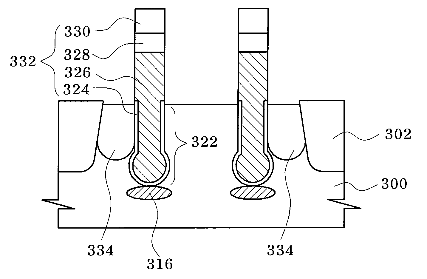
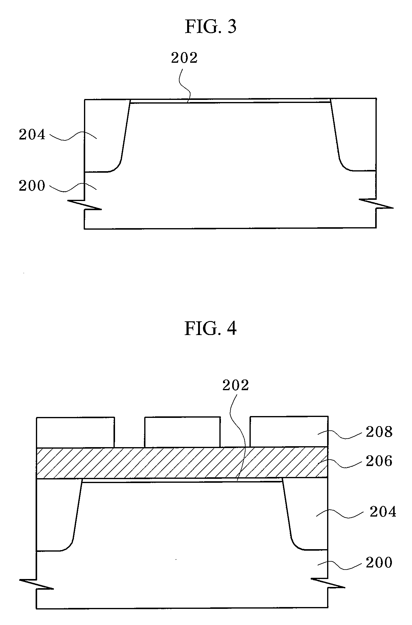
[0030]Referring to FIG. 3, a buffer film 202 for exposing device isolation regions of a semiconductor substrate 200 and a pad nitride film (not shown) are formed on the semiconductor substrate 200. An etching process of the exposed regions of the semiconductor substrate 200 is performed, thus forming trenches (not shown) having a designated depth in the semiconductor substrate 200. Th...


PUM


Abstract

A method for forming a semiconductor device having recess channel includes forming a hard mask film pattern for exposing first regions for forming the trenches on a semiconductor substrate; forming first trenches by a first etching process using the hard mask film pattern as a mask, and removing the hard mask film pattern; forming a barrier film on the semiconductor substrate including the first trenches; forming an ion implantation mask film for exposing the first trenches on the barrier film; forming an ion implantation region in the semiconductor substrate below the first trenches using the ion implantation mask film and the barrier film; forming bulb-shaped second trenches by a second etching process using the ion implantation mask film and the barrier film as a mask, so that bulb-type trenches for recess channels, each including the first trench and the second trench, are formed; and removing the ion implantation mask film and the barrier film.

Description

BACKGROUND OF THE INVENTION[0001]The present invention relates to a method for fabricating a semiconductor device and more particularly to a method for forming a semiconductor device having recess channels.[0002]As the degree of integration in an integrated circuit semiconductor device increases and design rules rapidly decrease, the difficulty in assuring the stable operation of transistors increases. For example, transistor gate widths and channel lengths are reduced rapidly. These causes short channel effects and can generate a punch through between the source and drain of the transistor. Punch through is one of the common reasons for the device malfunction. In order to overcome the short channel effect, various methods for assuring a sufficient channel length without increasing design rules have been developed. Particularly, a method for fabricating a semiconductor device having bulb-type recess channels using a two-stage etching process to increase the length of the channels in...

Claims


Application Information

Patent Timeline
Patent Type & Authority Applications(United States)
IPC IPC(8): H01L21/336
CPCH01L21/26586H01L29/4236H01L29/66621H01L29/66553H01L29/66537H01L21/18
Inventor LEE, JIN YULHA, MIN HOCHA, SEON YONG
Owner SK HYNIX INC
Why Eureka
Try Eureka