Atomic device

a technology of atomic devices and insulating plates, applied in nuclear engineering, separation processes, nanoinformatics, etc., can solve the problems of difficult shielding of magnetic fields, ohmic loss and thereby heat generation, and limitations of substrate integration, etc., to suppress the coupling of particles, good stability point, and long coherence time

Inactive Publication Date: 2007-07-12
JAPAN SCI & TECH CORP
View PDF4 Cites 15 Cited by
  • Summary
  • Abstract
  • Description
  • Claims
  • Application Information

AI Technical Summary

Benefits of technology

[0012] As can be seen from the Stark potential equation UE=−α|E|2/2, the aforementioned arrangement makes use of the second-order effect of the electric field to control a particle. This allows for suppressing the coupling of the particle being controlled by its environment or a disturbance. Accordingly, such an atomic device is realized which is resistant to decoherence.
[0013] In switching between the first state and the second state, it is preferable that the two electrodes of the second pair of electrodes be set at the reference potential in the first state, and the two electrodes of the first pair of electrodes be set at the reference potential in the second state. This makes it possible to create a good stable point at a position to be sandwiched by the two pairs of electrodes.
[0014] It is also preferable that the neutral particle trapped on the substrate for use be a neutral atom or a neutral molecule having no spin. For such a particle, a long coherence time can be expected with its quantum state. This is advantageous with respect to the extensibility of the atomic circuit.
[0015] Furthermore, it is preferable that, in the atomic device, a group of electrodes made up of the first pair of electrodes and the second pair of electrodes has an electrode spacing of 10 μm or less. An electrode structure provided

Problems solved by technology

However, such a conventional atom control technology has raised several problems with implementation of various atomic devices such as an atomic circuit that utilizes flows of atoms.
That is, in the aforementioned technology, a current is allowed to flow through a conductor wire on a substrate to control an atom, thus inevitably resulting in the occurrence of Ohmic loss and thereby heat generat

Method used


Image

  • Atomic device
  • Atomic device
  • Atomic device

Examples


Embodiment Construction

[0033] Preferred embodiments of the atomic device according to the present invention will be described below in detail with reference to the drawings. The same elements will be described by the same reference symbols in the description of the drawings, without redundant description. It is noted that the dimensional ratios in the drawings do not always agree with those in the description.

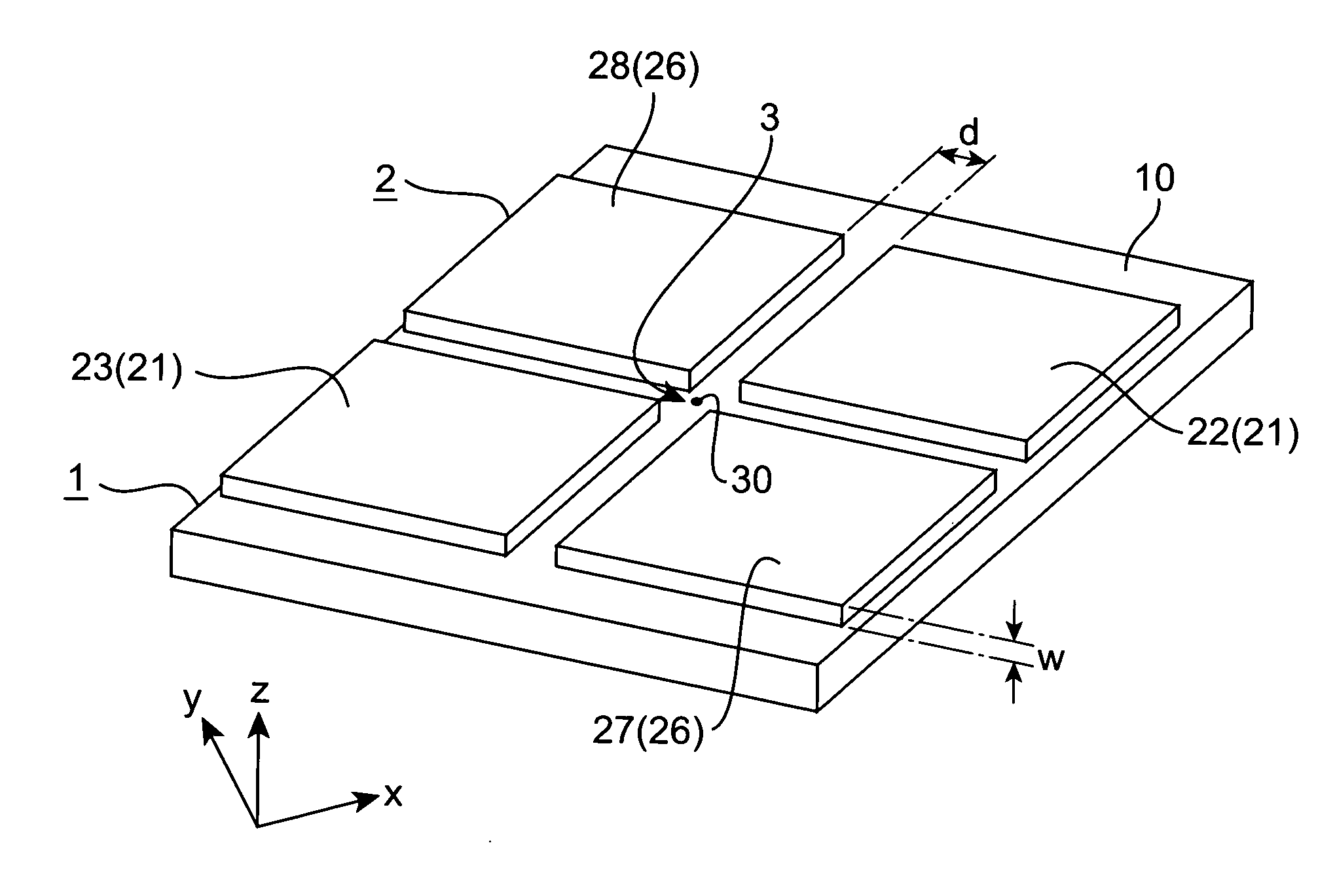
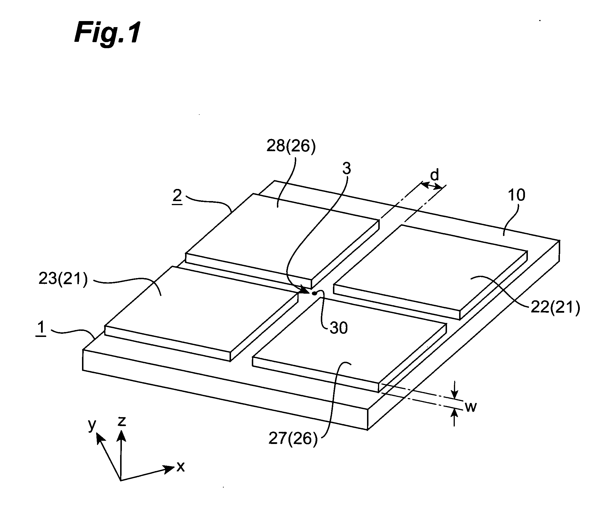
[0034]FIG. 1 is a perspective view illustrating the configuration of an embodiment of an atomic device according to the present invention. This atomic device is an atomic substrate (atom chip) which uses a neutral particle trapped on the substrate, and includes a substrate 1 and an electrode pattern 2. In the description below, such a case will be mainly illustrated where a neutral atom is employed; however, in general, a neutral atom or a neutral molecule can be employed as a neutral particle.

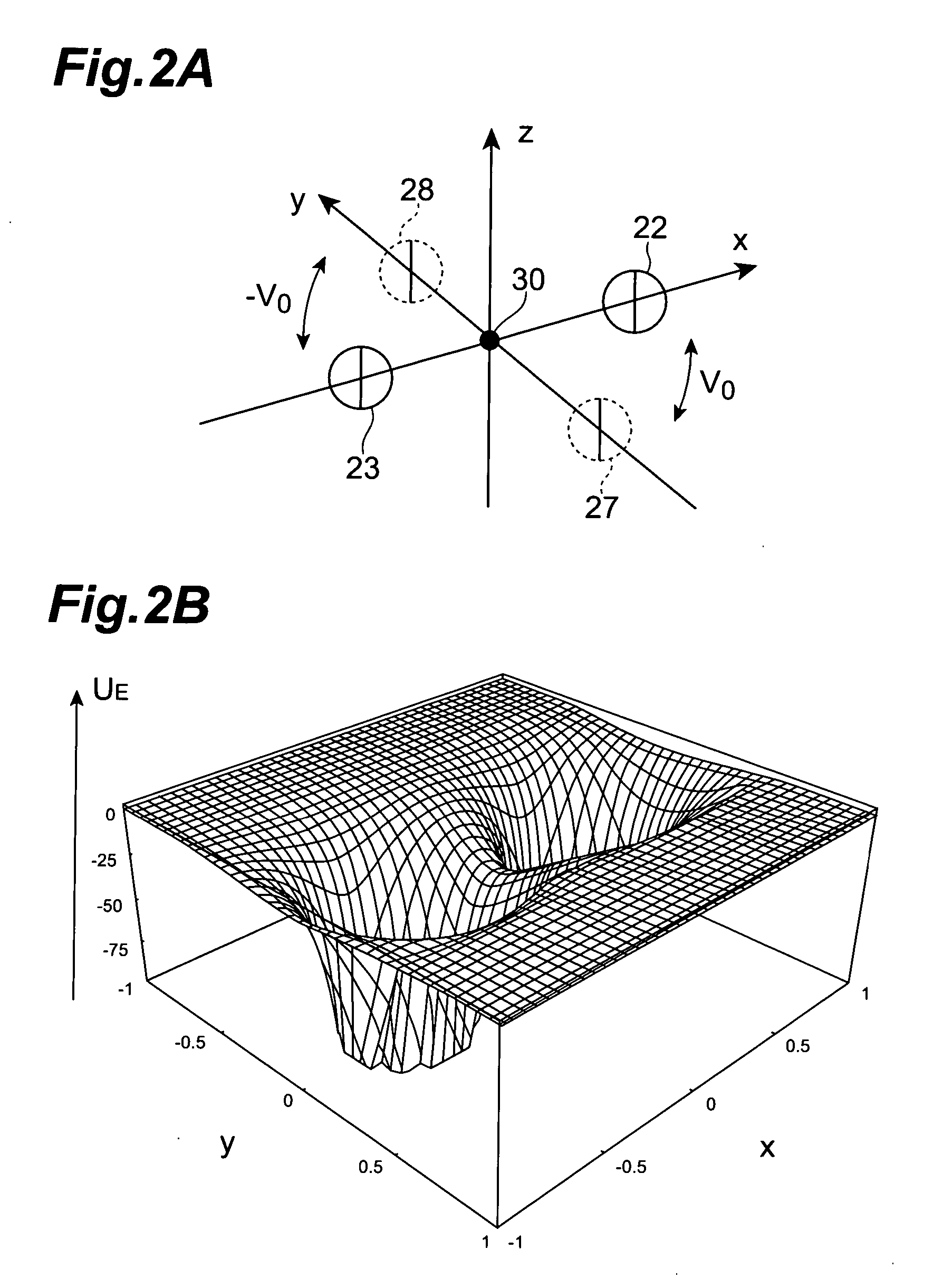
[0035] For convenience of description, a coordinate system including x, y, and z axes is defined as follow...


PUM


Abstract

A trapping position 30 is defined on a substrate 1, and an electrode pattern 2 is formed on the substrate 1, having a first pair of electrodes 21 including electrodes 22 and 23 formed at positions opposite each other with the trapping position 30 placed therebetween along a diagonal x-axis, and a second pair of electrodes 26 including electrodes 27 and 28 formed at positions opposite each other with the trapping position 30 placed therebetween along a y-axis orthogonal to the x-axis. The atomic device alternately switches between a first state and a second state to trap a neutral atom at the trapping position 30; in the first state, the electrode 22 of the first pair of electrodes 21 is set at a positive potential +V0 with respect to a reference potential and the electrode 23 is set at a negative potential −V0, and in the second state, the electrode 27 of the second pair of electrodes 26 is set at the positive potential +V0 and the electrode 28 is set at the negative potential −V0. This allows for realizing an atomic device which can facilitate integration of atomic circuits and reduce disturbances or the like.

Description

TECHNICAL FIELD [0001] The present invention relates to an atomic device in which a neutral atom or a neutral molecule is trapped on a substrate for use. BACKGROUND ART [0002] Conventional information processing technology has employed electronics technology in which use is made of electron flows and photonics technology in which photon flows are utilized. Recently, in contrast to this, discussions have focused on the possibility of realizing an “atomic circuit” in which controlled flows of atoms are coherently operated on a substrate. Like the development of electronics or photonics in which employed is sophisticated control of electrons or photons, such an atom control technology will be potentially developed as a new information processing technology which may be referred to as “atomtronics.”[0003] In particular, particles such as atoms or molecules for use with this technology have a larger number of degrees of interior or exterior freedom resulting from their complicated struct...

Claims


Application Information

Patent Timeline
IPC IPC(8): H01J49/00B82B1/00G21K1/00H01L29/06H01L29/788
CPCB82Y10/00H01L29/7888G21K1/006
Inventor KATORI, HIDETOSHI
Owner JAPAN SCI & TECH CORP
Why Eureka
Try Eureka