Inductor device for multiband radio frequency operation

a multi-band radio frequency and integrated circuit technology, applied in solid-state devices, amplifiers with semiconductor devices/discharge tubes, inductances, etc., can solve the problems of increasing complexity and die area consumption, not being able to implement multi-band operation in die-area effective practice, and increasing complexity and die-area consumption. , to achieve the effect of reducing the amount of different signal paths

Inactive Publication Date: 2007-07-12
NOKIA CORP
View PDF9 Cites 28 Cited by
  • Summary
  • Abstract
  • Description
  • Claims
  • Application Information

AI Technical Summary

Benefits of technology

[0009] The inductor device according to the invention can significantly decrease the amount of different signal paths required to cover all the different frequency bands by enabling use of a single passive inductor device, which is the most area consuming part in the RF front-ends, for all these different frequency bands. By this way, the RFIC chip is not including any totally unused inductor devices of an unused frequency resonator, but every large-area inductor is at least partially used. Further, in a differential distributed inductor according to the invention, the noise caused by the bypass switch is common-mode noise and thereby does not appear in the differential outputs of the inductor. This is an advantage in comparison to the prior art stacked inductor in which the MOSFET switch is on the current path and all noise energy caused by the switch is superimposed to the signal path. The differential distributed inductor according to the invention is directly a

Problems solved by technology

The future trend for multipurpose Radio Frequency Integrated Circuit (RFIC) implementations with multiple simultaneous systems and frequency bands in a telecommunication business is unquestionable.
This is setting demanding requirements for the RFIC engines with an increased complexity and die area consumption.
This is not a die-area effective practice to implement a multiband operation, since at least the other signal path is always shutted down as a dead di

Method used


Image

  • Inductor device for multiband radio frequency operation
  • Inductor device for multiband radio frequency operation
  • Inductor device for multiband radio frequency operation

Examples


Embodiment Construction

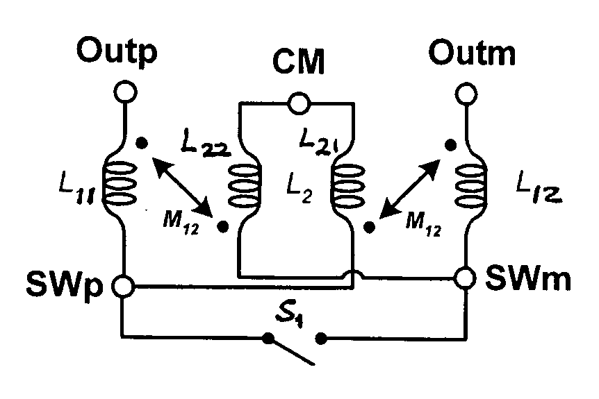
[0032] In FIG. 1, the basic idea of the invention is illustrated by means of an example. The inductance of a monolithic planar inductor is distributed into smaller inductor portions L11, L21, L22, and L12. The node CM between the immediate inductor portions L21 and L22 is a common-mode point of the inductor device, which is typically connected to the signal ground (e.g. to the supply voltage VCC or ground). The nodes Outm and Outp at the outer ends of the inductor portions L12 and L11 are differential outputs, e.g. output nodes of an amplifier device at the interface of the device itself and the following device (e.g. input stage of a mixer). The node SWp between the intermediate inductor portion L22 and the outer inductor portion L11 , and the node SWm between the intermediate inductor portion L21 and the outer inductor portion L12 are nodes where the shortcut switching function is implemented by means of a shortcut or bypass switching device S1 connected between the nodes SWp and ...


PUM


Abstract

The inductance of a monolithic planar inductor is distributed into smaller inductor portions. The smaller inductor portions are provided in a cascode configuration in a manner that causes inductor to function as a differential inductor device. The node between the immediate inductor portions is a common-mode point of the inductor device, which is typically connected to the signal ground. The nodes at the outer ends of the inductor portions are differential outputs, e.g. output nodes of an amplifier device at the interface of the device itself and the following device (e.g. input stage of a mixer). Some of the inductor portions are arranged to be symmetrically bypassed or shortcut in relation to the common point in one or more steps for operation in one or more higher radio frequency band. By means of the switchable symmetric shortcut, a controllable inductance step can be provided. The common-mode signal is affected the same inductance regardless of the controlled condition.

Description

FIELD OF THE INVENTION [0001] The present invention relates to radio-frequency (RF) circuits, and particularly to integrated circuits for multiband radio-frequency (RF) operation. BACKGROUND OF THE INVENTION [0002] The future trend for multipurpose Radio Frequency Integrated Circuit (RFIC) implementations with multiple simultaneous systems and frequency bands in a telecommunication business is unquestionable. New frequency allocations together with the frequency bands obtained from out-of-date commercial systems or government and military machineries create a very scattered radio interface. This is setting demanding requirements for the RFIC engines with an increased complexity and die area consumption. The overall degree of separate RF signal paths in a multi-purpose RFIC can be high and will be certainly increased in the future. For example, an RFIC for a mobile telephone may need to support GSM800, GSM1800, GSM1900, CDMA2000, European WCDMA, US WCDMA, WLAN, GPS, and DVB radio int...

Claims


Application Information

Patent Timeline
IPC IPC(8): H01L29/00H01FH01F17/00
CPCH01F17/0006H01F2017/0046H03F2203/45386H03F3/45098H01F2021/125
Inventor HEIKKINEN, JARI J.
Owner NOKIA CORP
Why Eureka
Try Eureka