Decentralized solution of microscopic particles and circuit formation device

a technology of microscopic particles and circuit formation devices, which is applied in the direction of microcapsules, non-conductive materials with dispersed conductive materials, record information storage, etc., can solve the problems of high cost, high cost, delay in delivery, etc., and achieve high speed, high thickness, and resolution without lowering

Inactive Publication Date: 2007-07-12
HITACHI LTD
View PDF15 Cites 5 Cited by
  • Summary
  • Abstract
  • Description
  • Claims
  • Application Information

AI Technical Summary

Benefits of technology

[0013]When a conductive microscopic particle decentralized solution according to the present invention is used in a printing process, a fine, low-resistance conductive pattern with a high thickness is obtained at high speed and at low heating temperature, without lowering the resolution.

Problems solved by technology

In addition, since a series of processes are complex, a long preparation time is needed, resulting in a high cost.
If it becomes necessary to modify the mask in, for example, limited production of a wide variety of products, a high cost, delayed delivery, and other problems occur.
The use of large quantities of materials hazardous to the environment, such as resists and etching solutions, is indispensable, so extra costs have been needed in management and processing of waste materials.
In the printing processes in which conductive patterns are formed by using a conductive microscopic particle decentralized solution in which conductive microscopic particles are decentralized, however, distances among microscopic particles in the conductive microscopic particle decentralized solution become large.
As a result, when conductive wires are formed by, for example, heating, many voids are generated and thereby the wires become more resistive and are weakened in strength.
To achieve the desired wire film thickness, films have to be laminated by repeating patterning, which may reduce the productivity.

Method used


Image

  • Decentralized solution of microscopic particles and circuit formation device
  • Decentralized solution of microscopic particles and circuit formation device
  • Decentralized solution of microscopic particles and circuit formation device

Examples


Embodiment Construction

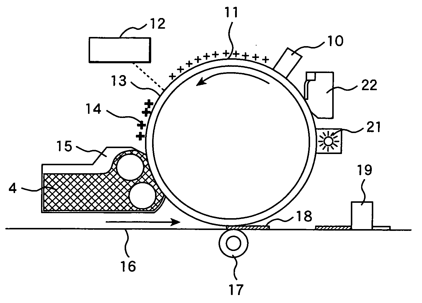
[0019]An embodiment of the present invention will be described below in detail.

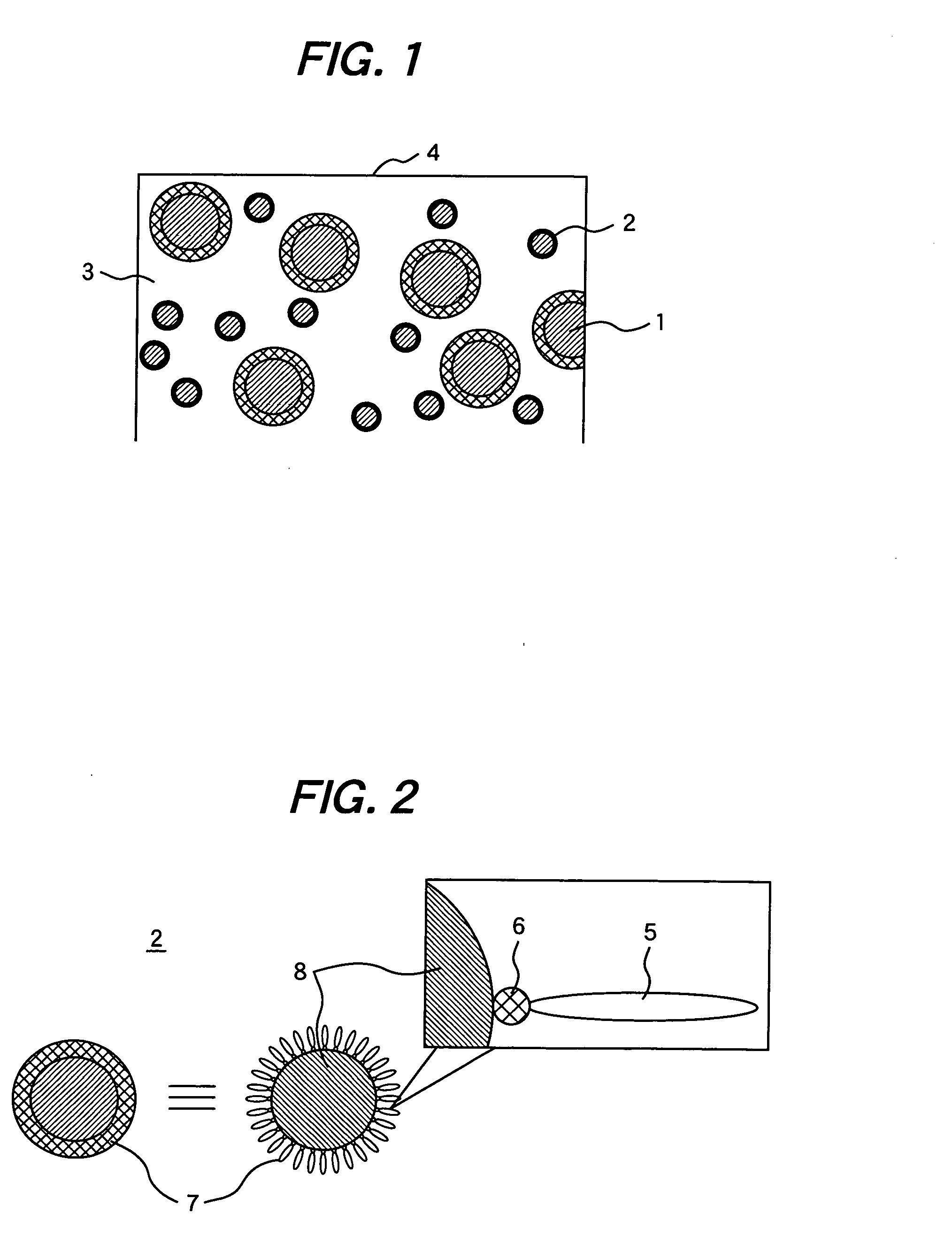
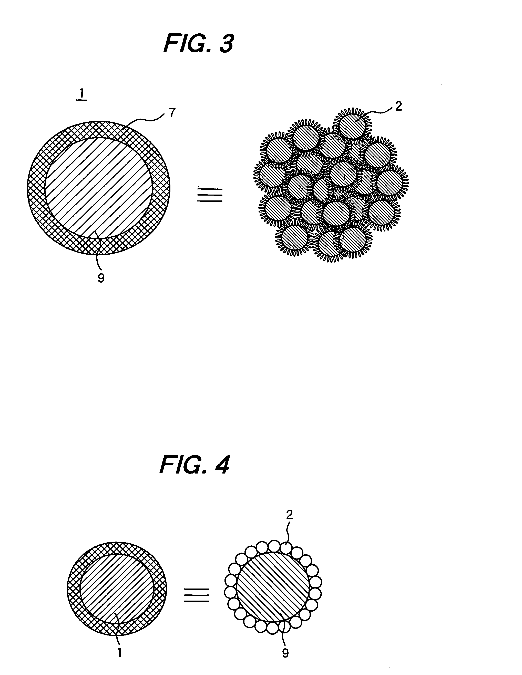
[0020]FIG. 1 shows a form of a conductive microscopic particle decentralized solution 4 proposed in the present invention. As shown in FIG. 1, in the conductive microscopic particle decentralized solution 4 proposed by the present invention, large-diameter particles 1 and small-diameter particles 2 decentralize concurrently in a decentralized solution 3. That is, the conductive microscopic particle decentralized solution 4 has two peaks in its granularity distribution, at a large diameter and a small diameter. The large-diameter particles 1 contribute to obtaining a higher thickness and increasing a pattern forming speed in conductive pattern formation, and the small-diameter particles 2 contribute to lowing the resistance of the conductive pattern and increasing the strength thereof in conductive pattern formation because the resolution is increased and the density of the conductive pattern is increased ...


PUM

PropertyMeasurementUnit
diameteraaaaaaaaaa
diameteraaaaaaaaaa
temperatureaaaaaaaaaa

Abstract

Microscopic particle decentralized solution having microscopic particles with different diameters are decentralized, wherein: the microscopic particle decentralized solution has two peaks in a granularity distribution, at a large diameter and a small diameter; and microscopic particle mixtures satisfying the following relationships are decentralized in the solution;
R>r and n>3.84×(R/r)3×N,
    • where R is a large particle diameter, r is a small particle diameter, N is the number of large particles, and n is the number of small particle.

Description

CLAIM OF PRIORITY[0001]The present application claims priority from Japanese application serial no. 2005-371282, filed on Dec. 26, 2005, the content of which is hereby incorporated by references into this application.BACKGROUND OF THE INVENTION[0002]1. Field of Technology[0003]The present invention relates to a decentralized solution of microscopic particles including nano-particle clusters and to a circuit formation device by using the decentralized solution of microscopic particles.[0004]2. Background of Art[0005]A conventional general method of forming arbitrary conductive patterns on a circuit board or the like is a method in which lithography technology, etching technology, and plating technology are combined. This method requires a mask for exposure that needs much time in designing and preparation as well as advanced machining technique. In addition, since a series of processes are complex, a long preparation time is needed, resulting in a high cost. If it becomes necessary t...

Claims


Application Information

Patent Timeline
Patent Type & Authority Applications(United States)
IPC IPC(8): G01N27/00
CPCH05K3/1266H05K2201/0224Y10T428/26H05K2203/0285H05K2203/0517H05K2203/0143
Inventor SANO, YUICHIROMIYASAKA, TORU
Owner HITACHI LTD
Why Eureka
Try Eureka