Structure of thin film transistor array and method for fabricating the same

a thin film transistor and array technology, applied in the direction of basic electric elements, electrical equipment, semiconductor devices, etc., can solve the problems of increasing fabrication costs, reducing fabrication costs, and more expensive masks, so as to reduce fabrication costs and simplify the process.

Inactive Publication Date: 2007-07-12
IND TECH RES INST
View PDF4 Cites 20 Cited by
  • Summary
  • Abstract
  • Description
  • Claims
  • Application Information

AI Technical Summary

Benefits of technology

[0010]According to the above description, an object of the present invention is to provide a structure of a TFT a

Problems solved by technology

Therefore, how to reduce the fabrication cost is the most concerned issue for manufacturers.
Moreover, the larger the panel substrate is, the more expensive the mask will be.
Accordingly, for fabricating the conventional TFT structure, five masks are inevitably required, which would increase the fabrication cost.
However, the half tone or gray tone mask is very expensive.
In this way, the fabricating cost cannot be significantly reduced.
Moreover, it i

Method used


Image

  • Structure of thin film transistor array and method for fabricating the same
  • Structure of thin film transistor array and method for fabricating the same
  • Structure of thin film transistor array and method for fabricating the same

Examples


first embodiment

The First Embodiment

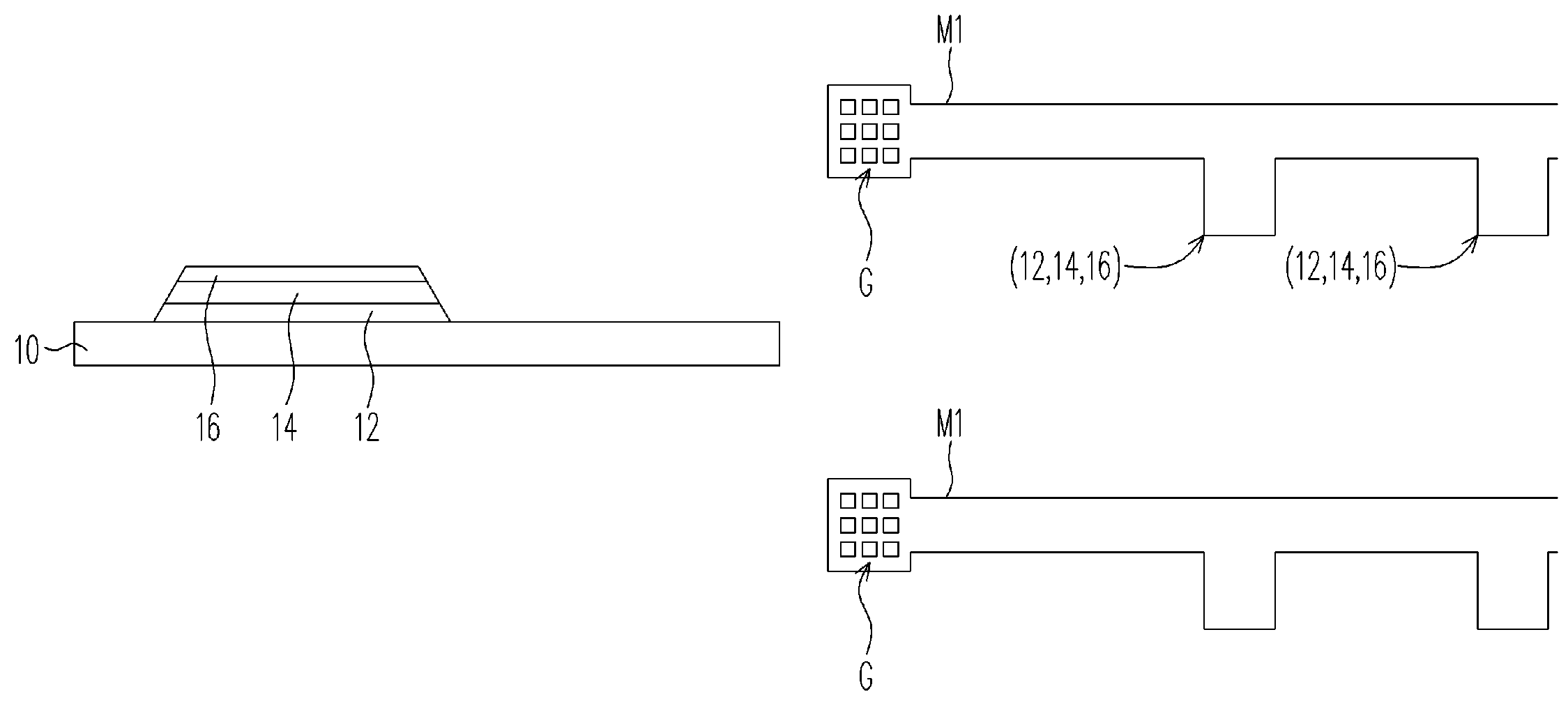
[0033]FIG. 3, FIGS. 4A to 4D, and FIG. 5 illustrate the first embodiment of the present invention. FIG. 3 is a cross-sectional view of the TFT fabricated using the fabricating method according to the first embodiment. FIGS. 4A to 4D are schematic views illustrating the process steps of fabricating method a TFT array according to the first embodiment of the present invention, in which the cross-sectional views shown at the left of each figure indicate the fabrication step, while the schematic views shown at the right side of each figure indicate the design of the display array. The left part of FIG. 5 is the schematic cross-sectional view of the gate pad or the gate line wiring area of the TFT in FIG. 3.

[0034]First, referring to FIG. 4A, a gate electrode layer 12, a gate insulating layer 14 and a silicon layer 16 are formed over the substrate 10. The substrate 10 can be any applicable substrate such as a glass substrate, a plastic substrate, a flexible substrate, ...

second embodiment

The Second Embodiment

[0045]FIG. 6, FIGS. 7A to 7D, and FIG. 8 illustrate the fabrication of a TFT array according to the second embodiment of the present invention. FIG. 6 is a cross-sectional view of the TFT fabricated using the method according to the second embodiment of the present invention. FIGS. 7A to 7D are schematic cross-sectional views illustrating the fabrication of the TFT array according to the second embodiment, wherein the cross-sectional views shown on the left of each figure indicate the fabrication step, while the schematic views shown on the right indicate the design of the TFT array. The left of FIG. 8 shows the schematic cross-sectional view of the gate pad or gate line wiring area of the TFT in FIG. 6.

[0046]As shown in FIG. 6, it is a variation embodiment of the first embodiment, and the difference between two embodiments is that the method for fabricating the source / drain. In the first embodiment, the method for fabricating the source / drain is the ion implant...


PUM


Abstract

A substrate having a gate electrode layer, a gate insulating layer, and a silicon layer thereon is provided. These layers are patterned into a gate area, a gate line and a gate line wiring area. A passivation layer is formed on the entire substrate and patterned to form two contact holes in the passivation layer on the silicon layer at the gate area, and partions of the passivation layer at the gate line and at the gate line wiring areas are removed. An ion implanting layer and a metal layer are formed on the substrate and patterned to form a source region, a drain region, a data line, a data line wiring area and a second layer of the gate line wiring area. A pixel electrode is formed on the passivation layer and electrically coupled to the drain region. Therefore, the TFT array can be fabricated by only four masks.

Description

CROSS-REFERENCE TO RELATED APPLICATION[0001]This application claims the priority benefit of Taiwan application serial no. 95101181, filed on Jan. 12, 2006. All disclosure of the Taiwan application is incorporated herein by reference.BACKGROUND OF THE INVENTION[0002]1. Field of the Invention[0003]The present invention relates to a structure of a thin film transistor (TFT) array and a method for fabricating the same. More particularly, the present invention relates to a structure of a TFT array and a method for fabricating the same by using four masks.[0004]2. Description of Related Art[0005]As going with the development of the flat panel display, the cost of thin film transistor liquid crystal displays (TFT LCDs) has been continuously reduced and the market share of TFT LCD has continuously increased. Therefore, how to reduce the fabrication cost is the most concerned issue for manufacturers. The fabrication of the current TFT array of a TFT LCD requires five masking processes, i.e.,...

Claims


Application Information

Patent Timeline
IPC IPC(8): H01L21/84H01L21/00
CPCH01L29/42384H01L27/1214H01L27/1248H01L27/1288
Inventor CHEN, YU-CHENG
Owner IND TECH RES INST
Why Eureka
Try Eureka