
Two-dimensional aperture array for vapor deposition

a technology of aperture array and vapor deposition, which is applied in the direction of vacuum evaporation coating, chemical vapor deposition coating, coating, etc., can solve the problems of affecting the masking precision of the carrier gas, the risk of decomposition of such materials, and the appreciable decomposition of organic materials. , to achieve the effect of eliminating the behavior of carrier gas underflow and high masking precision

Active Publication Date: 2007-07-19
GLOBAL OLED TECH
View PDF14 Cites 64 Cited by
  • Summary
  • Abstract
  • Description
  • Claims
  • Application Information

AI Technical Summary

Benefits of technology

[0033] (vi) Enables higher masking precision by eliminating carrier gas underflow behavior.

Problems solved by technology

For example, many organic semiconductor materials are not stable at high temperatures for a long period of time.
Depending on their decomposition characteristics, however, such heating can present the risk of decomposition for such materials.
In some cases, maintaining vapor sources at the temperatures required for vaporization for extended periods can cause appreciable decomposition of the organic material over long runs.
Conventional systems generally exhibit poor utilization, often wasting the majority of material.
Careful design and set-up of planetary motion substrate holders can make better use of the vaporized material, but this approach is generally limited to batches of a large number of very small substrates, so as to ensure nearly constant radial distance from substrate surface to point source.
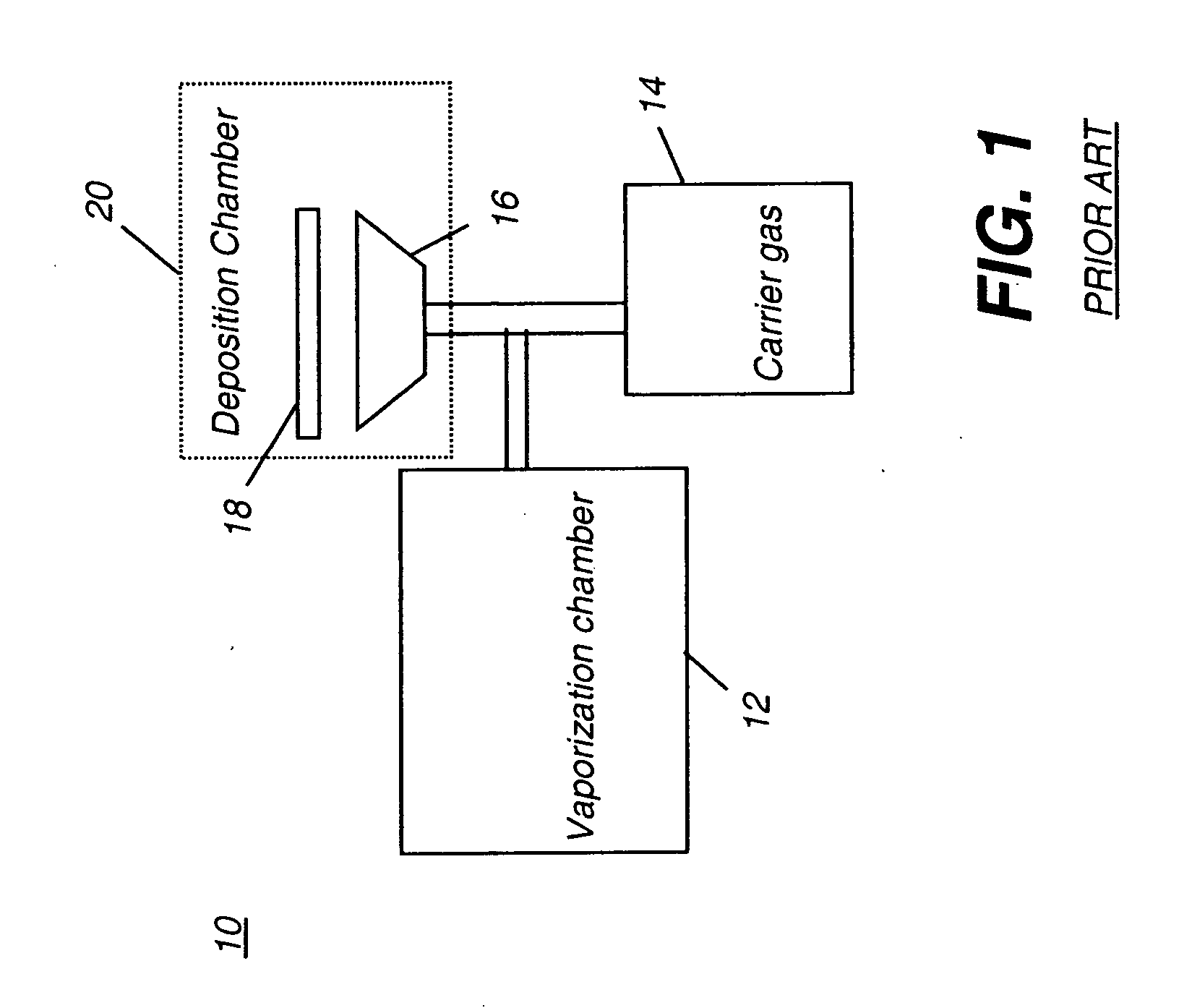
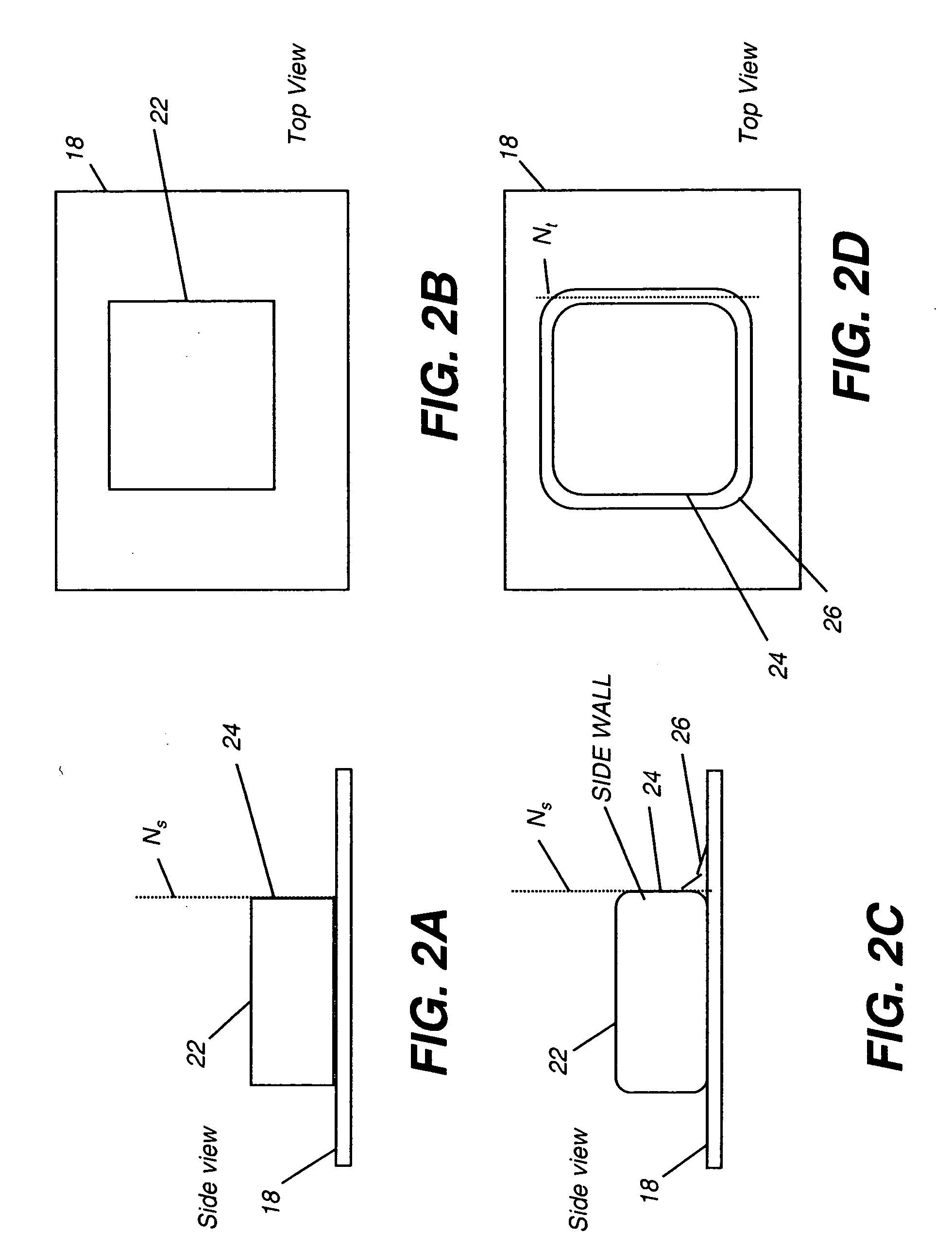
Another problem with CVD and OVPD systems relates to patterning precision when using shadow masks.
This vapor underflow is an undesirable side effect of viscous flow.
In component fabrication, this means that device resolution is limited as a result.
Yet another drawback of CVD and OVPD apparatus and methods relates to surface temperatures of the substrate.
With the advent of organic semiconductors and other organic electronic materials, and with the drive to fabricate devices on organic polymeric substrates, however, substrate temperature concerns are very different from those in the classical semiconductor industry, where the CVD approach has routinely been used to deposit inorganic dielectrics, metals, and semiconductors.
Deposition processes that operate in the viscous flow regime may cause significant substrate heating, owing to the thermal conductivity of the carrier gas or of the precursor or vaporized material, which transports heat from the exit surface of the heated gas delivery system (showerhead) to the substrate surface.
However, although the Chow et al.
Nor are there any guidelines given for scaling in order to adapt a given deposition system architecture for handling different substrate sizes.

Method used


Image

  • Two-dimensional aperture array for vapor deposition
  • Two-dimensional aperture array for vapor deposition
  • Two-dimensional aperture array for vapor deposition

Examples


example 1

Plume Shape Exponent p=1

[0085] For this example, Equation 3 was used to integrate the contributions from a square array of apertures of lateral extent l on a substrate surface of lateral extent L spaced a distance d therefrom (see FIGS. 10 and 11). The number n of apertures on each edge of length l of the array was specified and thus determined the total number of apertures and the corresponding pitch. The emission strength (intensity) of the four apertures on the corners and the emission strength (intensity) of the apertures on the outer edges (that is, along a line extending between the corner apertures) were specified and are respectively denoted Ic and Ie. Ic and Ie are emission strengths relative to the remaining apertures, which are assigned a strength value of unity in these examples. The spatial distribution of deposition rate was determined for the various geometry and emission strength parameters. Ic and Ie and were varied to produce the best deposition uniformity. The pl...

example 2

Plume Shape Exponent p=2

[0092] As in Example 1, Equation 3 was used to integrate the contributions from a square array of apertures of lateral extent l on a substrate surface of lateral extent L spaced a distance d therefrom. The same parameters were specified and the same calculations were performed using a value of 2 for the plume shape exponent p. In this case, the critical value of Pa d was found to be approximately 1.11 (as in the above example, this critical value is assessed by examining the local uniformity near the center of the substrate, edge effects notwithstanding). The results are tabulated in Table 3. The geometrical scaling relationships for utilization and emission strength for corners and edges are shown in FIGS. 20A and 20B. In addition, points tabulated in Table 4 show how the width e of the perimeter zone of enhanced aperture emission can be further increased to improve the uniformity, but at a cost of utilization (see FIG. 19). Furthermore, the emission streng...

example 3

Plume Shape Exponent p=3

[0095] As in Example 1, Equation 3 was used to integrate the contributions from a square array of apertures of lateral extent l onto a substrate surface of lateral extent L spaced a distance d therefrom. The same parameters were specified and the same calculations were performed using a value of 3 for the plume shape exponent p. In this case, the critical value of Pa d was found to be approximately 1.22. As in the earlier examples, this critical value is assessed by examining the local uniformity near the center of the substrate, edge effects not withstanding). The results of the calculations are tabulated in Table 5. The geometrical scaling relationships for utilization and emission strength for corners and edges are shown in FIGS. 21A and 21B.

TABLE 5#holesHoledonPitchCornerEdgeUnifL (cm)(cm)l (cm)edge(# / cm)e (cm)pP · dL4 / (d2el)CenterCenter(+ / −)Utiliz15.24216.49160.9100.62531.8191.31E+031.91.430.01480.66541004102.5330.3121.2531.2494.88E+041.361.220.03260....


PUM

PropertyMeasurementUnit
Massaaaaaaaaaa
Lengthaaaaaaaaaa
Lengthaaaaaaaaaa

Abstract

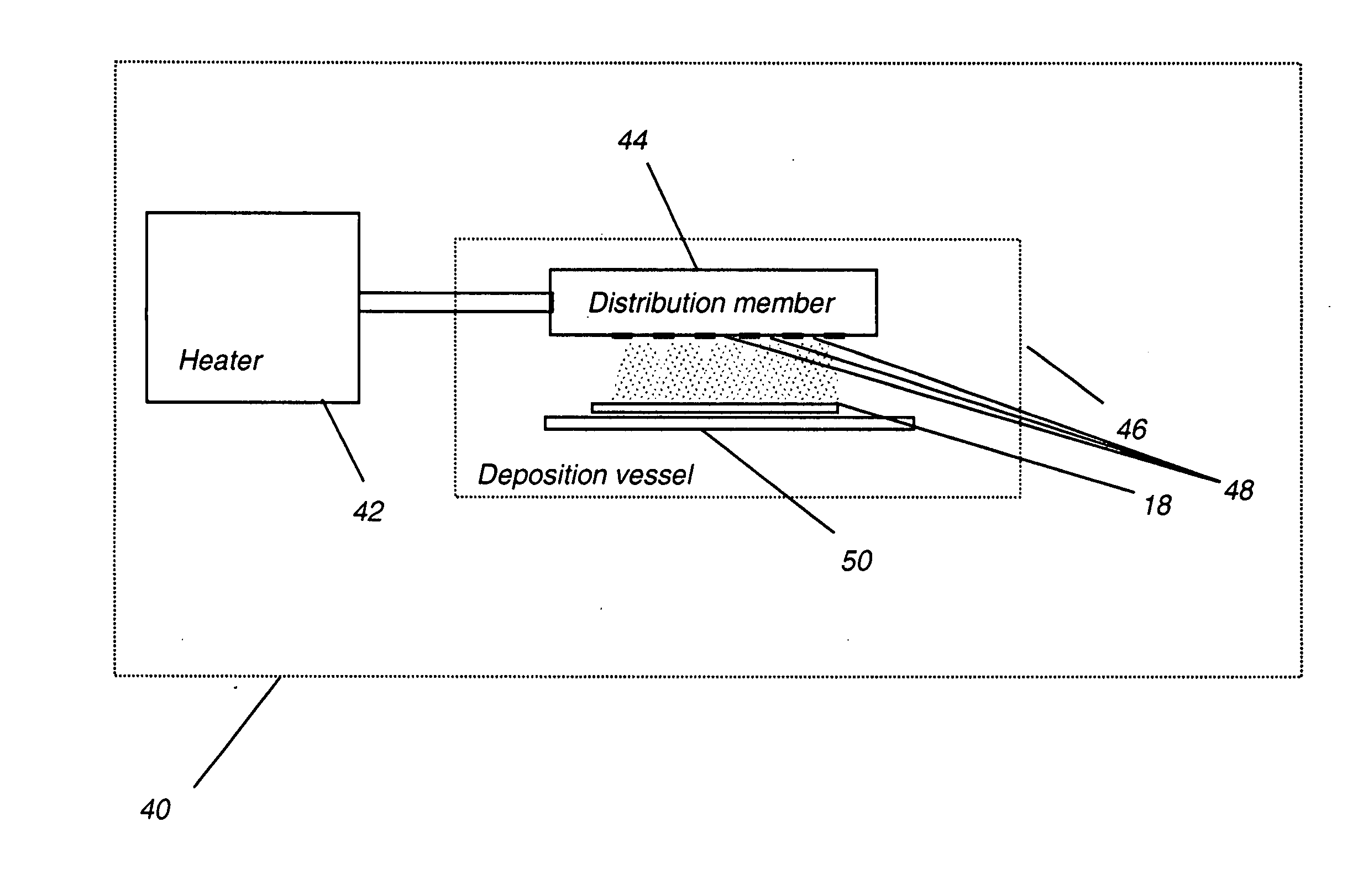
A method for forming a layer on a surface in making a device, including providing a distribution member for receiving vaporized material, the distribution member having one or more walls defining a polygonal two-dimensional pattern of apertures is formed in a wall, which deliver vaporized material in a molecular flow onto the surface; providing the polygonal two-dimensional pattern of apertures to have at least four vertices, with a first set of apertures disposed at the vertices, a second set of edge apertures disposed between the apertures of the first set and defining the edges of the polygonal two-dimensional pattern, and a third set of interior apertures disposed within the periphery of the polygonal two-dimensional pattern defined by the first and second sets of apertures; and dimensioning the apertures to obtain a desired flow rate.

Description

FIELD OF THE INVENTION [0001] This invention generally relates to deposition of thin films and more particularly relates to an apparatus and method for vapor deposition of a material in the molecular flow regime with optimized utilization and uniformity.BACKGROUND OF THE INVENTION [0002] The ongoing development of electronic and optical components has motivated the development of a variety of techniques for thin-film deposition of an ever-broadening array of materials. For semiconductor fabrication, for example, various methods of Chemical Vapor Deposition (CVD) have been developed for dielectric materials, metals and semiconductors. In CVD, a precursor material is delivered in vapor form and mixed with a carrier gas. This process gas mixture is then delivered to a substrate, either by expansion into a well-mixed process volume, or by localized distributed through a showerhead located near the substrate. The process pressures and geometries employed in CVD are generally selected to ...

Claims


Application Information

Patent Timeline
IPC IPC(8): C23C16/00
CPCC23C16/45565C23C14/044C23C16/455C23C16/00
Inventor GRACE, JEREMY M.LONG, MICHAEL
Owner GLOBAL OLED TECH
Learn More