Wireless IC device and component for wireless IC device

a wireless ic chip and wireless technology, applied in high-frequency circuit adaptations, instruments, high-level techniques, etc., can solve the problem of difficult mounting of wireless ic chips b>310, achieve sufficient gain, improve signal propagation efficiency, and improve antenna gain

Active Publication Date: 2007-07-19
MURATA MFG CO LTD
View PDF37 Cites 248 Cited by
  • Summary
  • Abstract
  • Description
  • Claims
  • Application Information

AI Technical Summary

Benefits of technology

[0011] With the wireless IC devices according to the first and second preferred embodiments of the present invention, the frequency of the transmission signal radiated from the radiation pattern, and the frequency of the reception signal supplied to the wireless IC chip are substantially determined by the resonant frequency of the resonant circuit in the power supply circuit board. The term “substantially determined” is used due to the frequency being minutely shifted due to the positional relationship between the power supply circuit board and the radiation pattern in some cases. That is to say, the frequencies of the transmission and reception signals are determined by the power supply circuit board, so that the frequency properties thereof are not changed regardless of the shape, size, and placement position of the radiation pattern, e.g., even if the wireless IC device is rounded, or sandwiched between dielectric members. Consequently, stable frequency properties are obtained.
[0037] The power supply portion and the power supply circuit pattern may be covered with a magnetic member. Thus, leakage of electromagnetic energy is prevented, and the coupling between the power supply portion and the power supply circuit pattern is improved, which produces improved antenna gain.

Problems solved by technology

However, it is extremely difficult to mount the wireless IC chip 310 on the large-area film 300 or 320.

Method used


Image

  • Wireless IC device and component for wireless IC device
  • Wireless IC device and component for wireless IC device
  • Wireless IC device and component for wireless IC device

Examples


first preferred embodiment

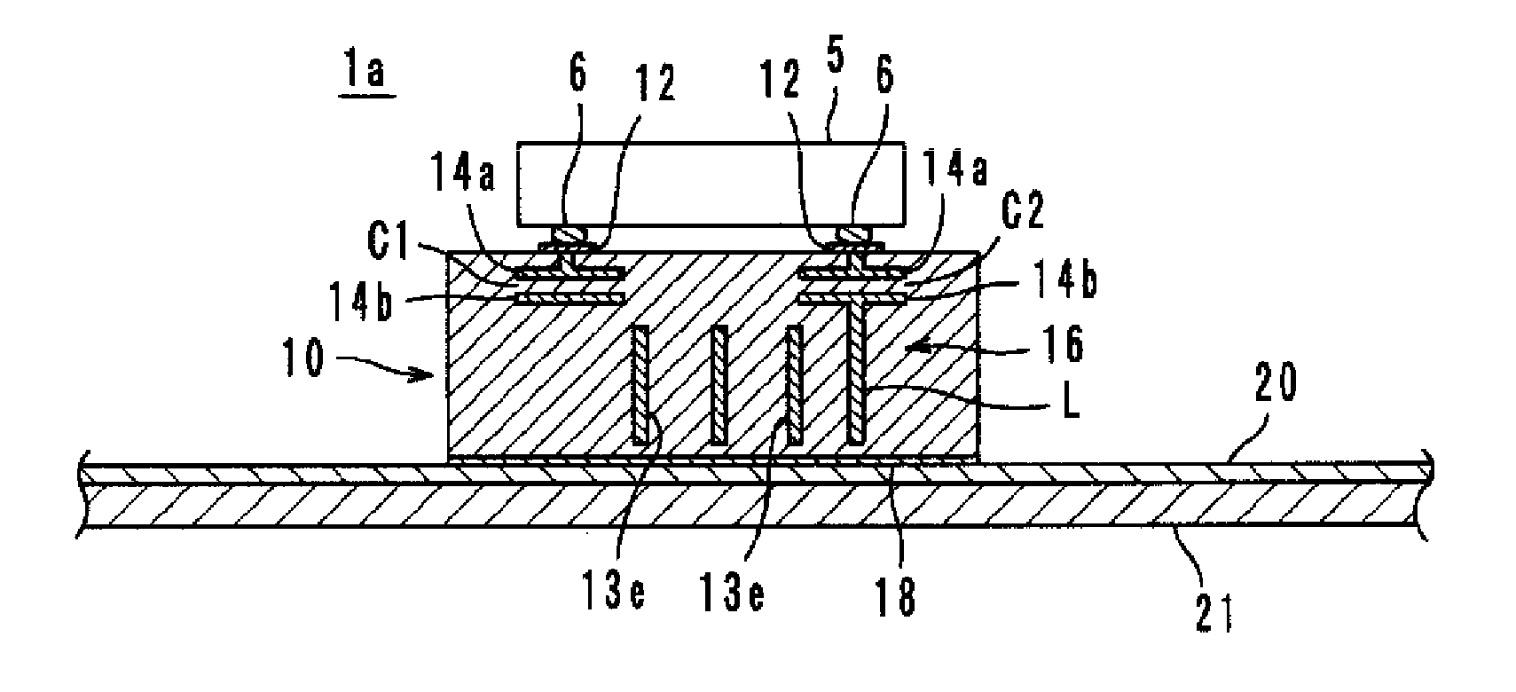
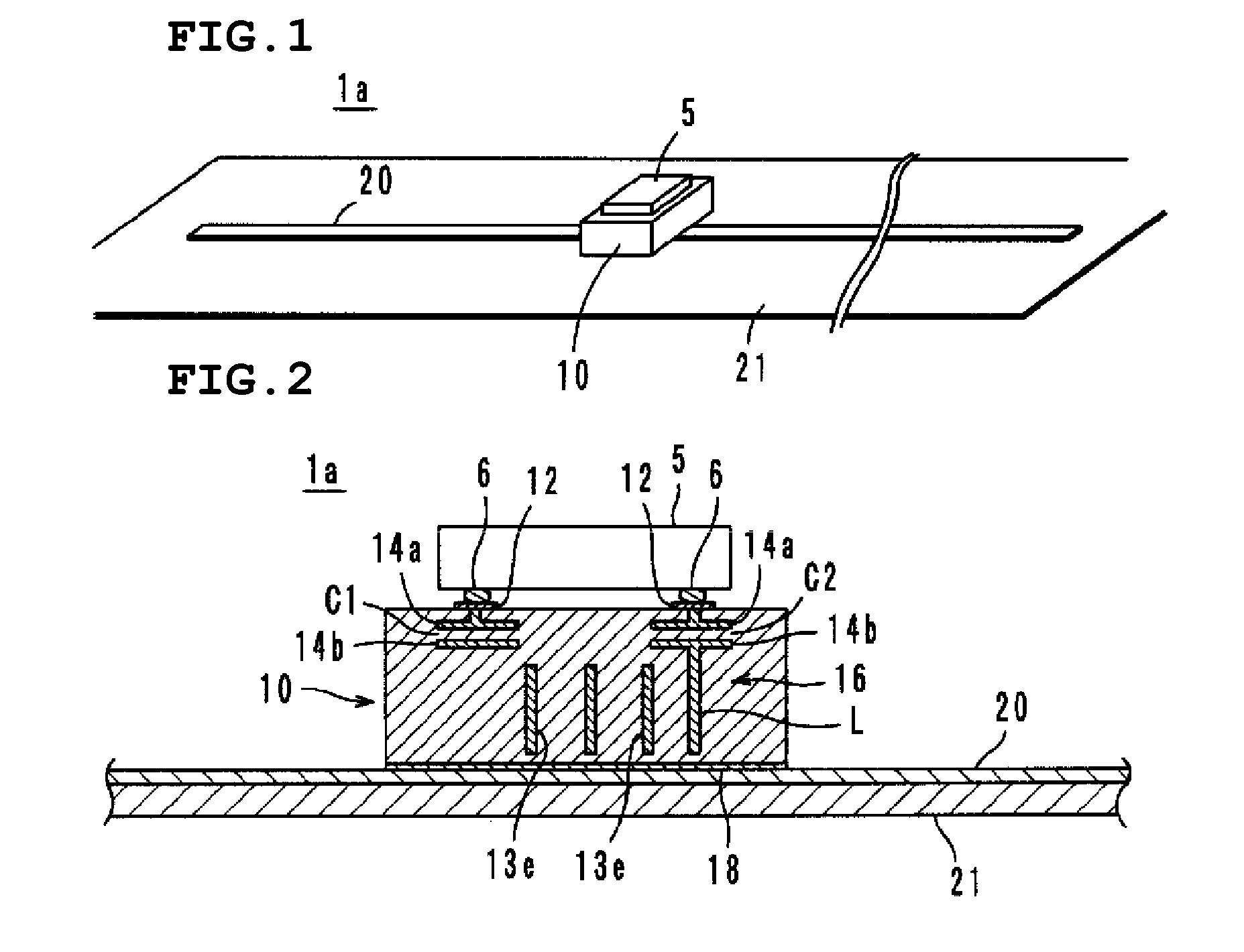
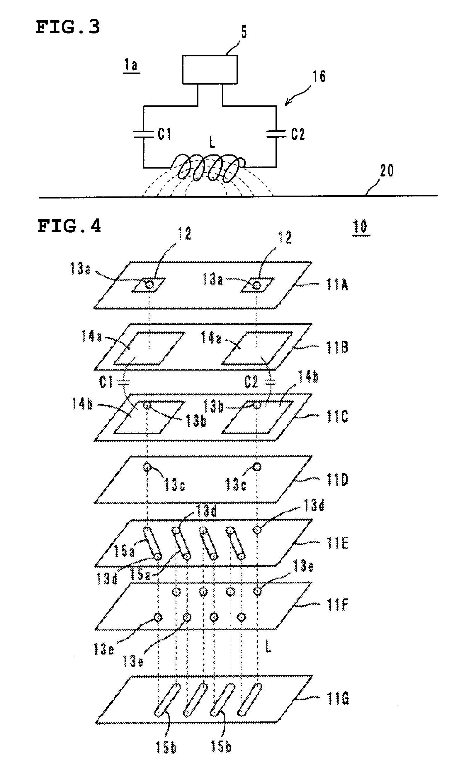
[0104] A wireless IC device 1a according to the first preferred embodiment is a monopole type, as illustrated in FIG. 1 and FIG. 2, and includes a wireless IC chip 5, a power supply circuit board 10 mounted on the wireless IC chip 5, and a radiation pattern 20 bonding the power supply circuit board 10. The wireless IC chip 5 includes a clock circuit, a logic circuit, and a memory circuit, stores necessary information therein, and is subjected to direct DC connection with a power supply circuit 16 provided in the power supply circuit board 10.

[0105] The power supply circuit 16 is a circuit for supplying a transmission signal having a predetermined frequency to the radiation pattern 20, and / or a circuit for selecting a reception signal having a predetermined frequency from signals received at the radiation pattern 20, and supplying it to the wireless IC chip 5, and includes a resonant circuit for resonating with the frequency of a transmission / reception signal.

[0106] As illustrated ...

second preferred embodiment

[0120] A wireless IC device 1b according to a second preferred embodiment is obtained by branching the radiation pattern 20 ninety degrees as shown in FIG. 8. That is to say, the radiation pattern 20 includes a radiation portion 20a extending in the X-axis direction within an x-y plane, and a radiation portion 20b extending in the Y-axis direction, a portion above the extension of the radiation portion 20a defines a power supply portion 20d, and the power supply circuit board 10, on which the wireless IC chip 5 is mounted, is adhered to the power supply portion 20d.

[0121] Note that the internal configuration of the power supply circuit board 10 is preferably the same as that in the first preferred embodiment, and the operations and advantages of the present second preferred embodiment are substantially the same as those in the first preferred embodiment. Further, the radiation portions 20a and 20b extend in the X-axis direction and Y-axis direction, whereby circularly-polarized wav...

third preferred embodiment

[0122] With a wireless IC device 1c according to a third preferred embodiment, as illustrated in FIGS. 9A and 9B, the radiation pattern 20 includes radiation portions 20a, 20b, and 20c extending in the X-axis direction, Y-axis direction, and Z-axis direction in x-y-z space, a portion above the extension of the radiation portion 20a defines a power supply portion 20d, and the power supply circuit board 10, on which the wireless IC chip 5 is mounted, is adhered to the power supply portion 20d.

[0123] The radiation pattern 20 of this wireless IC device 1c is adhered to a corner portion of a box-shaped article, the radiation portions 20a, 20b, and 20c extending three-dimensionally, so the directivity of the antenna is eliminated, and consequently, effective transmission / reception can be performed in any direction. Further, the other operations and advantages of the wireless IC device 1c are the same as those in the first preferred embodiment.


PUM


Abstract

A wireless IC device includes a wireless IC chip, a power supply circuit board upon which the wireless IC chip is mounted, and in which a power supply circuit is provided, the power supply circuit includes a resonant circuit having a predetermined resonant frequency, and a radiation pattern, which is adhered to the underside of the power supply circuit board, for radiating a transmission signal supplied from the power supply circuit, and for receiving a reception signal to supply this to the power supply circuit. The resonant circuit is an LC resonant circuit including an inductance device and capacitance devices. The power supply circuit board is a multilayer rigid board or a single-layer rigid board, and between the wireless IC chip and the radiation pattern is connected by DC connection, magnetic coupling, or capacitive coupling.

Description

BACKGROUND OF THE INVENTION [0001] 1. Field of the Invention [0002] The present invention relates to a wireless IC device, and particularly, to a wireless IC device used for an RFID (Radio Frequency Identification) system, and a component used for the wireless IC device. [0003] 2. Description of the Related Art [0004] In recent years, for an inventory item management system, an RFID system has been developed which includes a reader / writer for generating a dielectric magnetic field and an IC tag (hereafter, referred to as wireless IC device) for storing predetermined information about an inventory item which communicate with one another via a non-contact method, thereby transmitting information. Known wireless IC devices used in RFID systems are described in Japanese Unexamined Patent Application Publication No. 2005-136528 (Patent Document 1) and Japanese Unexamined Patent Application Publication No. 2005-244778 (Patent Document 2), for example. [0005] The wireless IC device shown i...

Claims


Application Information

Patent Timeline
Patent Type & Authority Applications(United States)
IPC IPC(8): H01L23/02
CPCG06K19/07749H01L2224/16235H01L23/642H01L23/645H01L23/66H01L2223/665H01L2223/6677H01L2224/13144H01L2224/16H01L2924/01079H01L2924/09701H01L2924/14H01L2924/3011H05K1/0239H05K1/0243H05K1/16H05K1/162H05K1/165H05K2201/10098H05K2201/10727H01L23/49822H01L2224/16238Y02D30/70
Inventor DOKAI, YUYAKATO, NOBORUISHINO, SATOSHI
Owner MURATA MFG CO LTD
Why Eureka
Try Eureka