
High-withstand voltage wide-gap semiconductor device and power device

a technology of wide-band semiconductors and power devices, applied in semiconductor devices, basic electric elements, electrical appliances, etc., can solve the problems of small losses and greatly reduced turn-on resistance, and achieve the effect of suppressing the increase of stacking faults and rising forward-direction voltag

Inactive Publication Date: 2007-07-26
THE KANSAI ELECTRIC POWER CO
View PDF2 Cites 79 Cited by
  • Summary
  • Abstract
  • Description
  • Claims
  • Application Information

AI Technical Summary

Benefits of technology

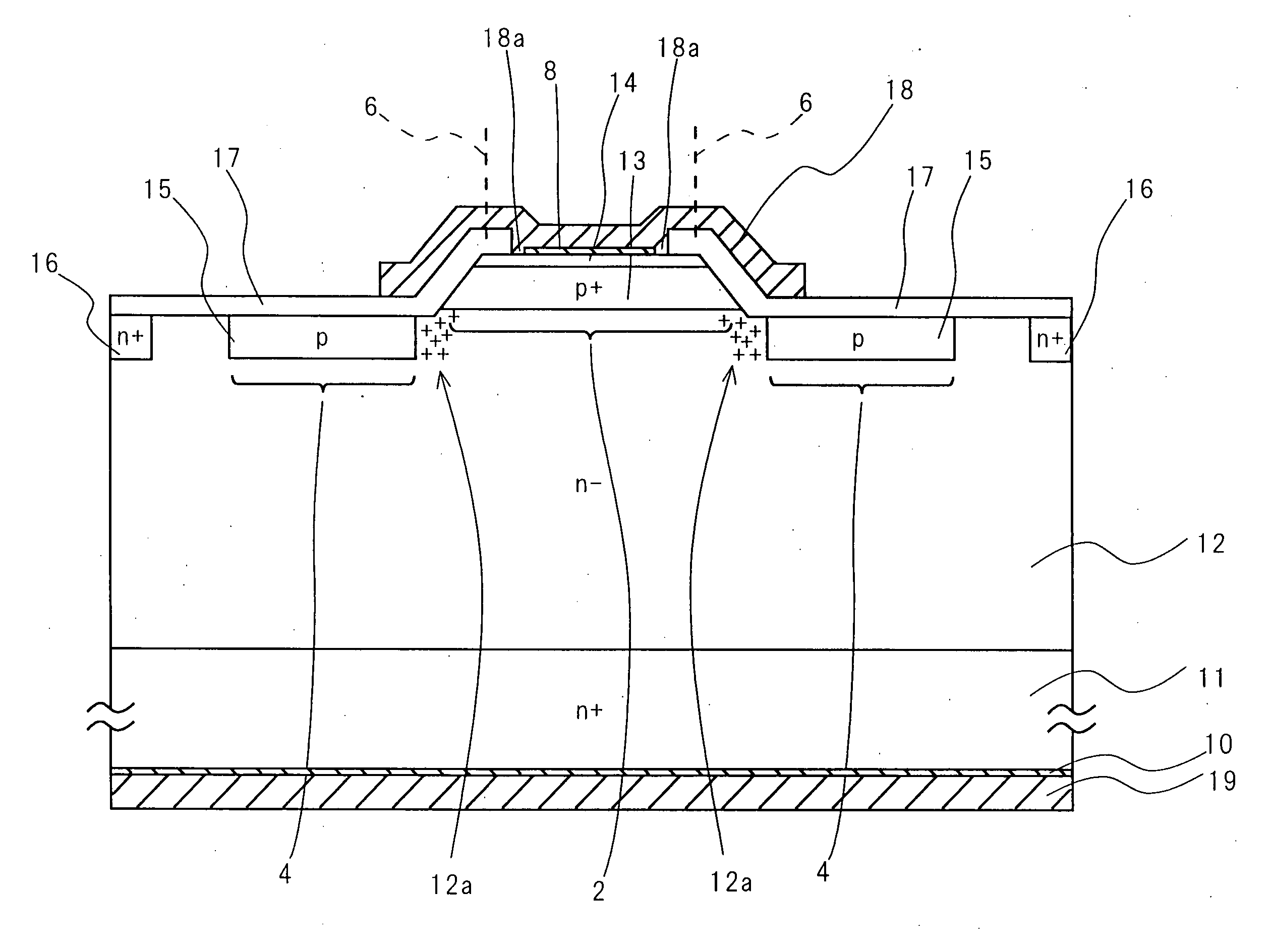
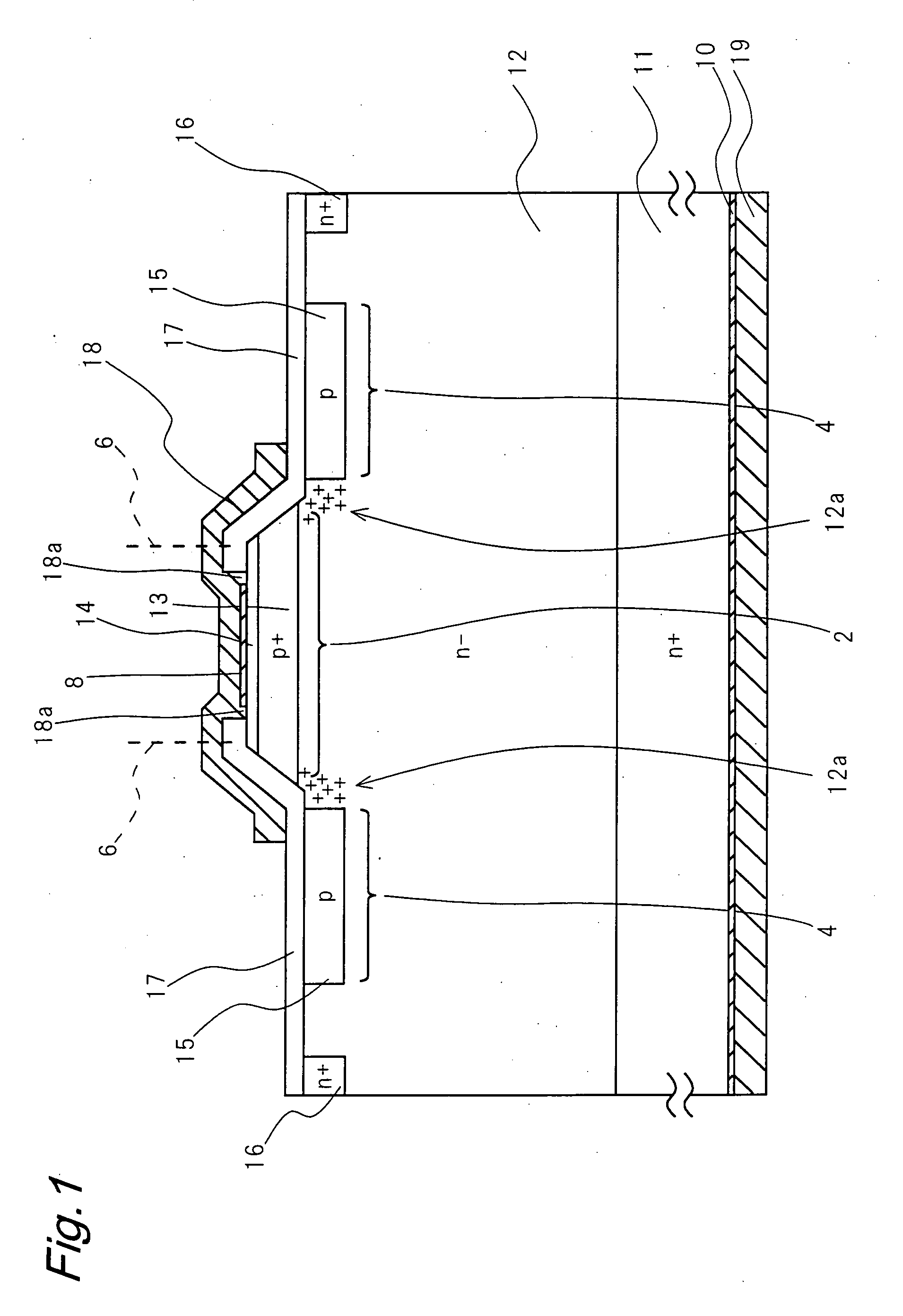
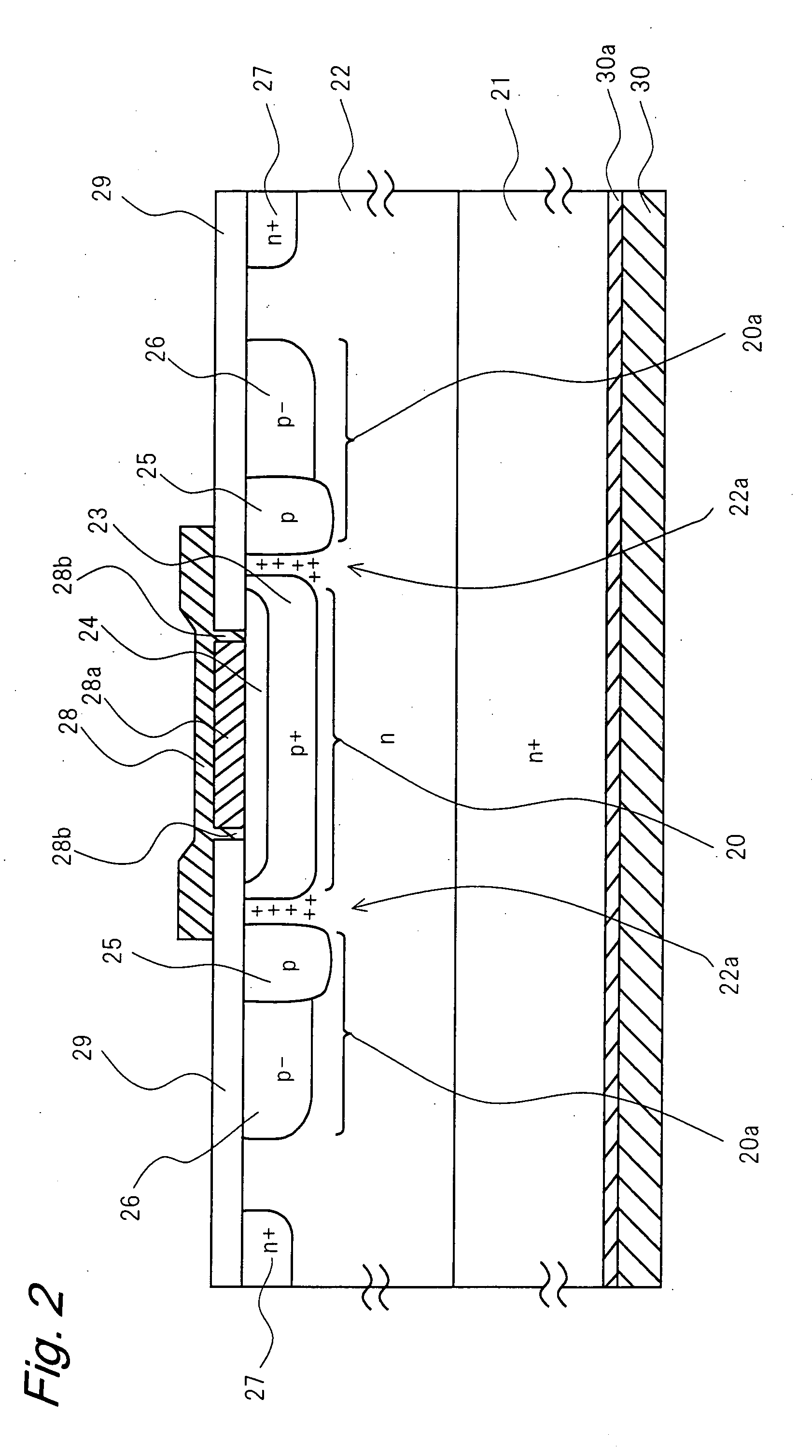
[0032] According to this invention, stacking faults which occur when a forward-direction current is flowing in a wide-gap semiconductor device are formed primarily in the portion of the semiconductor region in which the forward-direction current is flowing, and so growth and expansion of stacking faults can be suppressed, and rises in forward-direction voltage due to increases in stacking faults can be suppressed.

Problems solved by technology

Moreover, because the turn-on resistance is greatly reduced due to conductivity modulation in the drift layer due to minority carrier injection, losses are small.

Method used


Image

  • High-withstand voltage wide-gap semiconductor device and power device
  • High-withstand voltage wide-gap semiconductor device and power device
  • High-withstand voltage wide-gap semiconductor device and power device

Examples


first embodiment

[0065]FIG. 1 is a cross-sectional view of a mesa-structure SiC PIN junction diode, which is the high-withstand voltage wide-gap semiconductor device of a first embodiment of the invention. In the figure, an n−-type SiC semiconductor drift layer 12 of thickness 75 μm and with impurity concentration 1×1014 cm−3 is formed, by epitaxial growth techniques, on a substrate 11 of n+-type SiC semiconductor, with impurity concentration 1×1019 cm−3, which acts as a cathode of thickness 400 μm. On the lower surface of the substrate 11 is provided a cathode electrode 19 (second electrode) of gold, copper or similar, with an Ohmic contact layer 10 intervening to maintain a satisfactory state of electrical contact. On the drift layer 12 are formed, in order, a p+-type SiC semiconductor anode layer 13, with impurity concentration 1×1018 cm−3 and thickness 1.5 μm, and a p+-type SiC semiconductor contact layer 14, with impurity concentration 1×1019 cm−3 and thickness 0.2 μm, using epitaxial growth te...

second embodiment

[0076]FIG. 2 is a cross-sectional view of a planar-structure SiC PIN junction diode, which is the semiconductor device of a second embodiment of the invention. In the figure, an n-type SiC drift layer 22, with impurity concentration 5×1014 cm−3 and of thickness 50 μm, is formed by epitaxial growth techniques on an n+-type SiC substrate 21, with impurity concentration 1×1019 cm−3 and of thickness 400 μm, operating as a cathode. In the center region of the drift layer 22, ion implantation techniques are used to form a p+-type SiC anode layer 23, with impurity concentration 1×1018 cm−3 and of thickness 0.5 μm, and a p+-type SiC contact layer 24, with impurity concentration 1×1019 cm−3 and of thickness 0.2 μm. A function 20 (first pn junction) is formed between the anode layer 23 and the drift layer 22.

[0077] Further, p−-type SiC JTE layers 25, with impurity concentration 8×1017 cm−3, of thickness 0.8 μm and length in the lateral direction approximately 25 μm, are provided at a distanc...

third embodiment

[0085]FIG. 3 is a cross-sectional view of a mesa-structure SiC GTO which is the high-withstand voltage, wide-gap semiconductor device of a third embodiment of the invention. In the figure, a p-type SiC buffer region 33 is formed on the upper surface of the substrate 32, comprising an n+-type SiC emitter region, and having a cathode 31 (second electrode) on the lower surface. On the buffer region 33 is formed a p−-type SiC base region 34; in the center of the base region 34 is formed a mesa-structure n-type SiC base layer 35. A junction 30 (first pn junction) is formed between the base region 34 and the base layer 35. Four gate electrodes 40 are provided in the base layer 35. The four gate electrodes 40 are connected at a portion not shown in the figure. A p-type SiC emitter layer 36 is formed between each of the gate electrodes 40.

[0086] The n+-type SiC substrate 32 has an impurity concentration of 1×1019 cm−3, and a thickness of 300 μm. The buffer region 33 has an impurity concent...


PUM


Abstract

A semiconductor device with high withstand voltage, reduced forward-direction voltage degradation, long lifetime and high reliability, is provided. A junction between the drift layer and anode layer of a bipolar semiconductor device and an electric field relaxation layer are formed at a distance from each other, and an edge portion of the anode is opposed to the semiconductor region between the junction and the electric field relaxation layer, with an insulating film intervening. When reverse-biased, due to the electric field effect imparted to the drift layer between the junction and the electric field relaxation layer from the electrode, with the insulating film intervening, the junction and electric field relaxation layer are electrically connected, and electric field concentration at the junction edge portion is relaxed. When forward-biased, the junction and electric field relaxation layer are electrically isolated, and forward-direction current flows only through the junction.

Description

TECHNICAL FIELD [0001] This invention relates to a wide-gap semiconductor device, and in particular relates to a high-withstand voltage wide-gap semiconductor device having a high withstand voltage, and to a power device having this semiconductor device. BACKGROUND ART [0002] Silicon carbide (SiC) and other wide-gap semiconductor materials have excellent characteristics, including a dielectric breakdown electric field intensity which is approximately ten times higher than for silicon (Si), and so are attracting attention as materials suitable for high-withstand voltage power semiconductor devices having high withstand-voltage characteristics. [0003] PIN diodes, bipolar transistors, GTOs and other bipolar semiconductor devices using wide-gap semiconductor materials have higher built-in voltages than that of unipolar semiconductor devices such as Schottky diodes and MOSFETs. Moreover, because the turn-on resistance is greatly reduced due to conductivity modulation in the drift layer d...

Claims


Application Information

Patent Timeline
Patent Type & Authority Applications(United States)
IPC IPC(8): H01L31/0312H01L29/06H01L29/74H01L29/12H01L29/24H01L29/40H01L29/417H01L29/744H01L29/78H01L29/861
CPCH01L29/0615H01L29/0619H01L29/0657H01L29/407H01L29/861H01L29/41716H01L29/41741H01L29/744H01L29/7811H01L29/417H01L29/872H01L29/1608
Inventor SUGAWARA, YOSHITAKA
Owner THE KANSAI ELECTRIC POWER CO
Learn More