Non-volatile memory with power-saving multi-pass sensing

a non-volatile memory and multi-pass technology, applied in static storage, digital storage, instruments, etc., can solve the problems of less accurate sensing and more power consumption of pre-charged components

Active Publication Date: 2007-07-26
SANDISK TECH LLC
View PDF33 Cites 18 Cited by
  • Summary
  • Abstract
  • Description
  • Claims
  • Application Information

AI Technical Summary

Benefits of technology

[0039] According to one aspect of the invention, power-saving in a sensing cycle for a page of memory cells is effected by minimizing the draining effect of the memory cells during a precharge operation. This is accomplished by first charging the bit lines without coupling to the memory cells. After the bit lines have been charged to a predetermined degree will the memory cells be coupled thereto to reach a final steady state condition before sensing is to take place.
[0040] According to another aspect of the present invention, power-saving in a sensing cycle for a page of memory cells is effected by reducing the precharge period before the actual sensing. Before sensing is to take place, the voltages on the word line and the bit lines need be set up by a precharge operation. The precharge operation consumes power and yet must be of sufficient duration so that the voltages will become sufficient stable before accurate sensing can take place. The invention calls for reducing the precharge period even beyond the point where the voltages are no longer sufficiently stable for accurate sensing relative to an original reference level. This is applicable in a sensing cycle which completion takes more than one sensing sub-cycle. When the precharge in the first sub-cycle consumes more power than a subsequent sub-cycle, and the precharge period of the first is reduced to save power at the expense of the subsequent sub-cycle, overall power is saved among the two sub-cycles.
[0041] In a preferred embodiment, a first sensing sub-cycle is employed to identify the highest current states so that they could be removed from the page being sensed in order to minimize any ground loop or source bias errors. With the high current cells of the page turned off, a second sensing sub-cycle will be able to sense the remaining cells of the page with better accuracy. Since the precharge for setting up the first sensing sub-cycle consumes relative more power due to the presence of more of the higher current cells, this precharge period is reduced to save power. The prematurely shortened precharge period, before the bit lines voltage has stabilized will result in less accurate sensing. In order not to erroneously detect the lower current cells as high current cells due to the presence of transient displacement currents before the bit line stabilized, the discrimination current level is set higher to provide a safe margin. This will result in detecting less of the higher current cells as compared to sensing after the bit line voltage has stabilized. Those higher current (intermediate conducting) cells that should have been detected but fail to be detected would be caught in a subsequent second sensing sub-cycle. However, their cell current was not turned off and would make the precharge drain more power in the second sub-cycle. It will also introduce a bit more ground loop bias voltage error during the second sensing.

Problems solved by technology

The prematurely shortened precharge period, before the bit lines voltage has stabilized will result in less accurate sensing.
However, their cell current was not turned off and would make the precharge drain more power in the second sub-cycle.

Method used


Image

  • Non-volatile memory with power-saving multi-pass sensing
  • Non-volatile memory with power-saving multi-pass sensing
  • Non-volatile memory with power-saving multi-pass sensing

Examples


Embodiment Construction

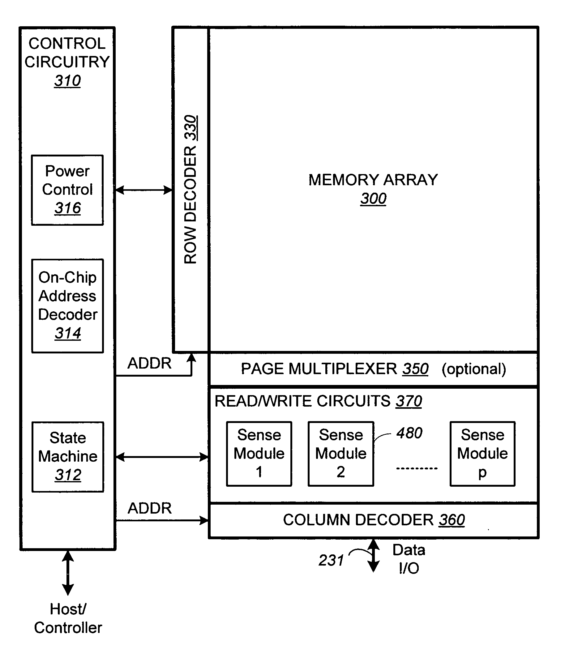
[0075]FIG. 6A illustrates schematically a compact memory device having a bank of read / write circuits, which provides the context in which the present invention is implemented. The memory device includes a two-dimensional array of memory cells 300, control circuitry 310, and read / write circuits 370. The memory array 300 is addressable by word lines via a row decoder 330 and by bit lines via a column decoder 360. The read / write circuits 370 is implemented as a bank of sense modules 480 and allows a block (also referred to as a “page”) of memory cells to be read or programmed in parallel. In a preferred embodiment, a page is constituted from a contiguous row of memory cells. In another embodiment, where a row of memory cells are partitioned into multiple blocks or pages, a block multiplexer 350 is provided to multiplex the read / write circuits 370 to the individual blocks.

[0076] The control circuitry 310 cooperates with the read / write circuits 370 to perform memory operations on the me...


PUM


Abstract

A non-volatile memory device capable of reading and writing a large number of memory cells with multiple read / write circuits in parallel has features to reduce power consumption during sensing, which is included in read, and program / verify operations. A sensing verify operation includes one or more sensing cycles relative to one or more demarcation threshold voltages to determine a memory state. In one aspect, coupling of the memory cells to their bit lines are delayed during a precharge operation in order to reduced the cells' currents working against the precharge. In another aspect, a power-consuming precharge period is minimized by preemptively starting the sensing in a multi-pass sensing operation. High current cells not detected as a result of the premature sensing will be detected in a subsequent pass.

Description

CROSS REFERENCE TO RELATED APPLICATION [0001] This application is related to an application being filed concurrently herewith by Shouchang Tsao et al., entitled “Method for Power-Saving Multi-Pass Sensing in Non-Volatile Memory” which application is incorporated herein in its entirety by this reference. FIELD OF THE INVENTION [0002] This invention relates generally to non-volatile semiconductor memory such as electrically erasable programmable read-only memory (EEPROM) and flash EEPROM, and specifically ones implementing optimizations for multi-pass sensing during read and program verify operations. BACKGROUND OF THE INVENTION [0003] Solid-state memory capable of nonvolatile storage of charge, particularly in the form of EEPROM and flash EEPROM packaged as a small form factor card, has recently become the storage of choice in a variety of mobile and handheld devices, notably information appliances and consumer electronics products. Unlike RAM (random access memory) that is also soli...

Claims


Application Information

Patent Timeline
Patent Type & Authority Applications(United States)
IPC IPC(8): G11C7/02
CPCG11C7/06G11C7/12G11C2211/5621G11C16/3418G11C11/5642
Inventor TSAO, SHOU-CHANGLI, YAN
Owner SANDISK TECH LLC
Why Eureka
Try Eureka