Debugging system for gate level IC designs

a gate level ic and design technology, applied in the field of integrated circuit design system, can solve problems such as difficulty in debugging, and achieve the effects of simplifying the debugging process, facilitating design understanding, and facilitating comprehension

Active Publication Date: 2007-07-26
SYNOPSYS INC
View PDF18 Cites 46 Cited by
  • Summary
  • Abstract
  • Description
  • Claims
  • Application Information

AI Technical Summary

Benefits of technology

[0010] In accordance with one aspect of the invention, the gate level dump file is processed to produce an RTL dump file referencing signals of the hierarchical RTL design, rather than of the gate level design, and indicating how those signals would behave in response to the time-varying signals supplied as inputs to the IC. A debugger then processes the RTL dump file to produce displays depicting the RTL design and the behavior of signals of the RTL design indicated by the RTL dump file. The gate level-to-RTL dump file conversion process enables the designer to debug the RTL design, rather than the gate level design, based on the gate level simulation or emulation or results. Since the hierarchical RTL design is easier for a designer to understand than the flat gate level design, the invention helps simplify the debugging process.
[0011] In accordance with another aspect of the invention, the output of an IC tester indicating IC signal behavior is converted into an RTL level dump file referencing signals of the IC's original RTL design and depicting the behavior of those signals during the test. A debugger then processes the RTL dump file to produce displays correlating the RTL design to the behavior of signals of the RTL design. The tester output-to-RTL dump file conversion process enables a test engineer to debug the hierarchical RTL level of the design based on test results, which is typically easier to comprehend than the flat gate level design.

Problems solved by technology

However, when the designer or test engineer uses debugger 16 of FIG. 1 or debugger 26 of FIG. 2 to review simulation, emulation or IC test results, the debugger 16 or 26 correlates the signal behavior described by dump file 14 or test data 26 to the gate level design which is more complicated and less familiar to the designer or test engineer, and therefore more difficult to debug.

Method used


Image

  • Debugging system for gate level IC designs
  • Debugging system for gate level IC designs
  • Debugging system for gate level IC designs

Examples


Embodiment Construction

[0018] The invention relates to a system for debugging an integrated circuit (IC) design and this portion of the specification describes a preferred mode of practicing the invention. Although the description below includes numerous details in order to provide a thorough understanding of that particular mode of practicing the invention, it will be apparent to those of skill in the art that other modes of practicing the invention recited in the claims need not incorporate all such details.

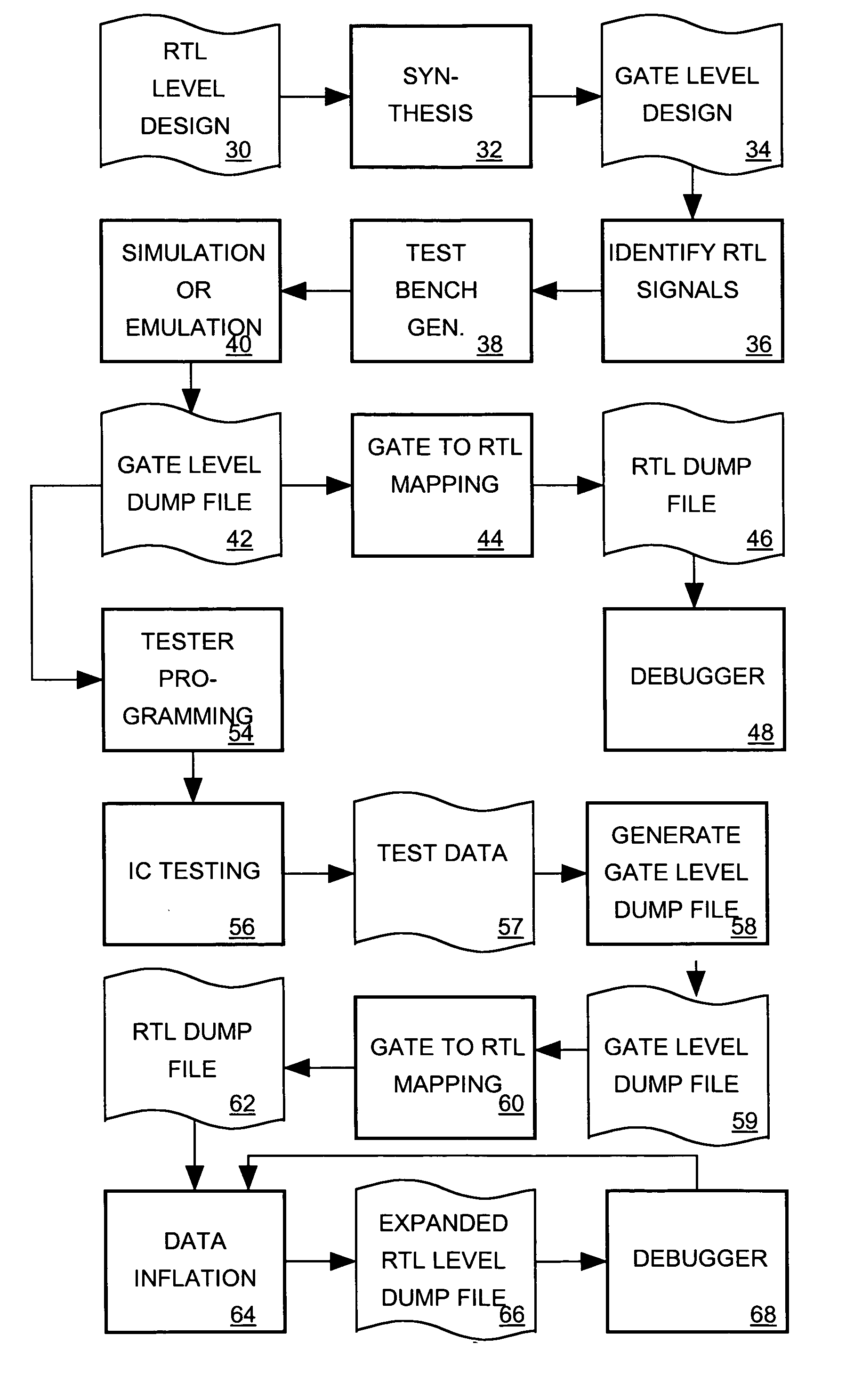
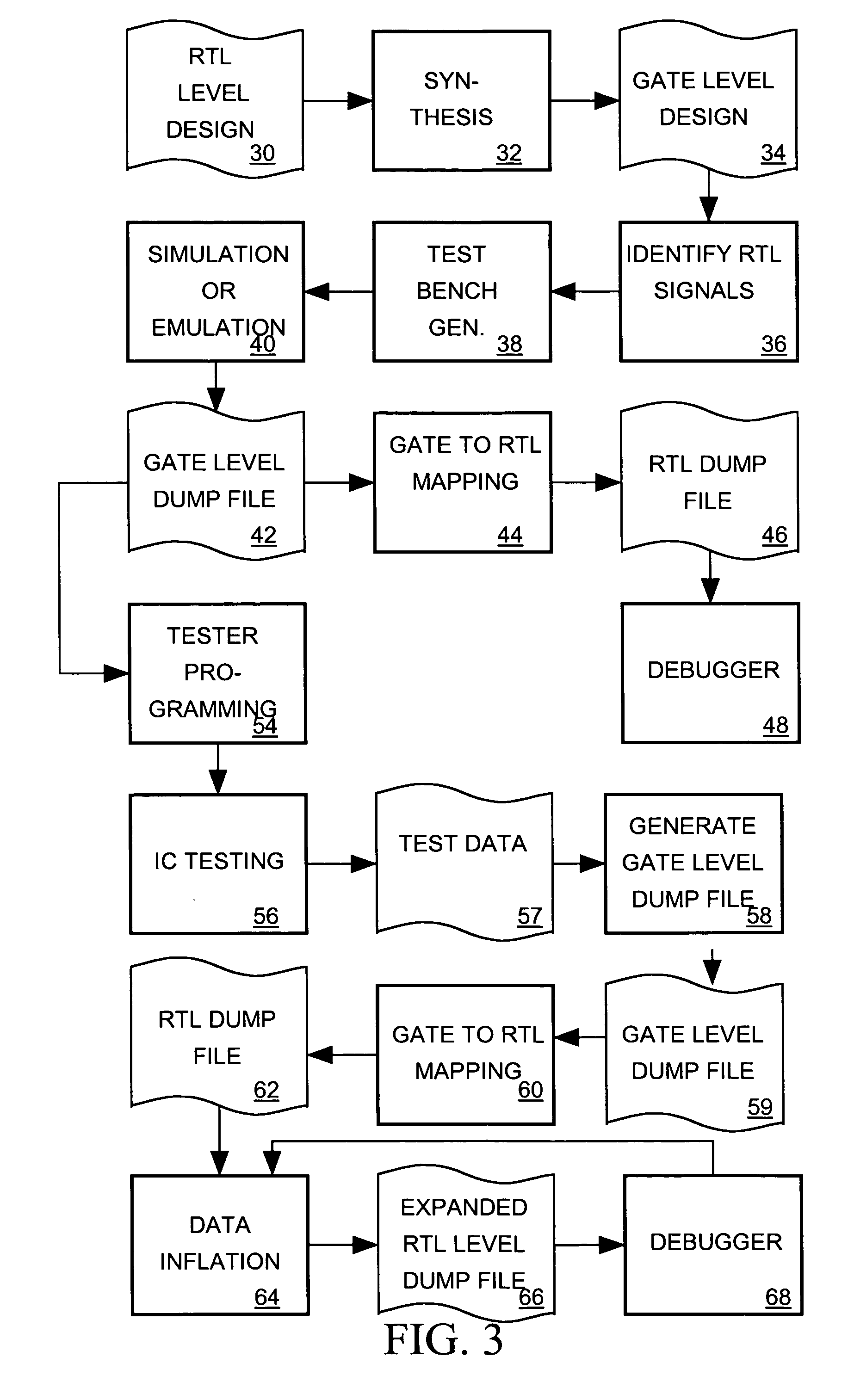
[0019]FIG. 3 is a data flow diagram illustrating an IC development process employing a debugging method in accordance with invention. An IC designer initially generates a text based register transfer level (RTL) IC design 30. A digital IC employs clocked devices such a registers, latches and flip-flops to synchronize state changes in signals between various blocks of logic to clock signal edges. A designer can think of an IC as being a hierarchy of logic modules for producing output signals as logic...


PUM


Abstract

A register transfer level (RTL) IC design describing a IC as comprising a plurality of logic blocks communicating via signals and using a high level language to describe the logic blocks according to the logical relationships between signals they receive and signals they generate. A computer-aided synthesizer processes an RTL IC design to produce a gate level design for the IC describing its logic blocks as comprising instances of cells communicating via signals. A synthesizer or emulator processes the gate level design to produce a gate level dump file referencing signals of the gate level design and indicating how those signals behave in response to time-varying signals supplied as inputs to the IC. The gate level dump file is converted into an RTL dump file referencing signals of the RTL design and indicating how those signals behave. A debugger processes the RTL dump file to produce displays depicting the RTL design and behavior of signals indicated by the RTL dump file. Thus while the IC is simulated or emulated at the gate level of the design to produce waveform data for a debugger, the gate level-to-RTL dump file conversion process enables a designer debug the more familiar RTL design based on the gate level simulation or emulation results.

Description

BACKGROUND OF THE INVENTION [0001] 1. Field of the Invention [0002] The invention relates in general to a system for debugging an integrated circuit (IC) design, and in particular to a debugging system that relates gate level simulation, emulation or IC testing results to a register transfer level design. [0003] 2. Description of Related Art [0004] An IC designer initially creates a “register transfer level” (RTL) design, also called a “register transfer logic” design, describing a digital electronic circuit as a hierarchy of logic modules that transmit data signals to one another via registers or other clocked devices that store information between clock cycles. The RTL design typically uses high level expressions to describe the logical relationships between the input and output signals of each block of logic. [0005] The designer uses a computer-aided synthesis tool to convert the RTL design into a gate level design describing the IC as a set of interconnected instances of compone...

Claims


Application Information

Patent Timeline
Patent Type & Authority Applications(United States)
IPC IPC(8): G06F17/50
CPCG06F17/5022G06F30/33
Inventor HSU, YU-CHINTSAI, FURSHINGJONG, WORI-TZY
Owner SYNOPSYS INC
Why Eureka
Try Eureka