Vapor deposition system and vapor deposition method for an organic compound

a technology of vapor deposition system and organic compound, which is applied in vacuum evaporation coating, electroluminescent light source, coating, etc., can solve the problems of high manufacturing cost, low throughput in mass production, and inability to form a wide film thickness distribution, etc., and achieve high material use efficiency

Inactive Publication Date: 2007-08-02
CANON KK
View PDF7 Cites 137 Cited by
  • Summary
  • Abstract
  • Description
  • Claims
  • Application Information

AI Technical Summary

Benefits of technology

[0015]By changing the shape of the openings in the opening member, fluctuation of the vapor deposition rate is compensated, and the film thickness distribution

Problems solved by technology

Because, on the other hand, the light emitting characteristics of an organic EL device depends on the thickness of the organic compound layer forming the device, it is not allowable that a wide film thickness distribution is formed on the surface of the substrate.
Therefore, the manufacturing cost is high and the throughput in mass production is low.
Further, as the manufacturing apparatus becomes larger, the cost of equipment increases.
However, even according to the method disclosed in Japanese Patent Application Laid-Open No. 2001-93667, there is a problem in that the material use efficiency is sacrificed.
The reason is that, beca

Method used


Image

  • Vapor deposition system and vapor deposition method for an organic compound
  • Vapor deposition system and vapor deposition method for an organic compound
  • Vapor deposition system and vapor deposition method for an organic compound

Examples


example 1

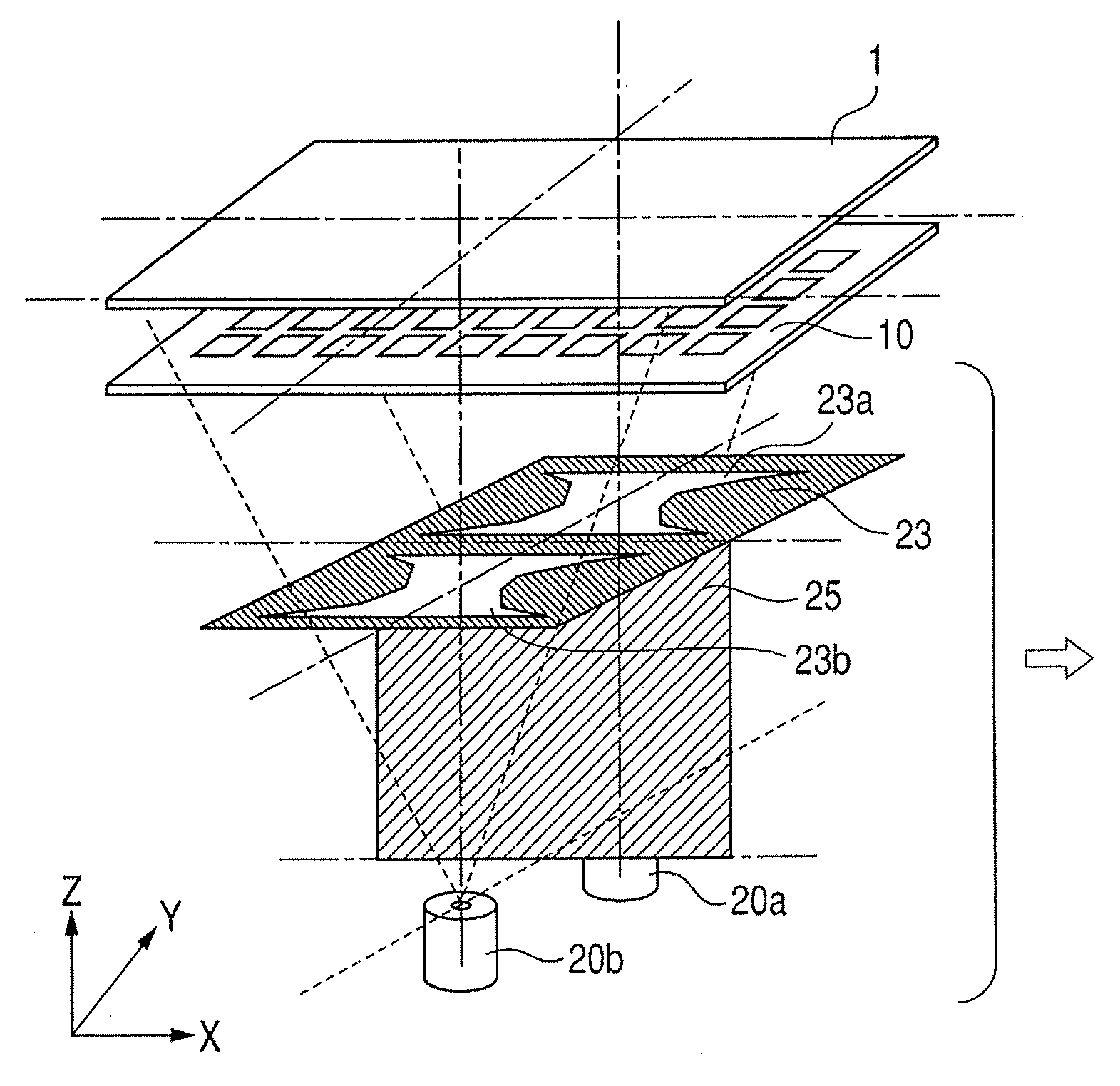
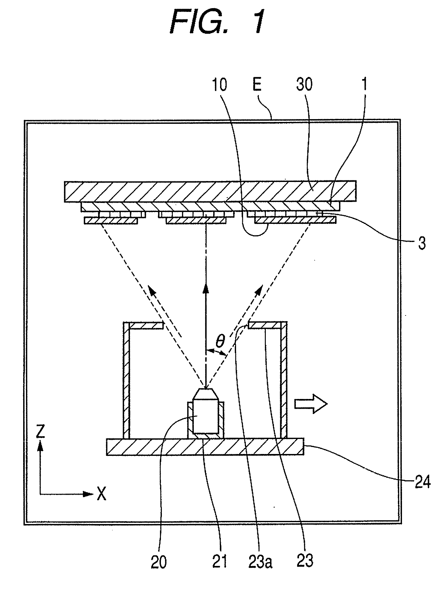
[0071]The system illustrated in FIG. 2 was used to manufacture an organic light emitting device. The substrate 1 of 400 mm×500 mm was used. The substrate 1 was placed such that the width direction thereof was in parallel with the X direction. The distance between the vapor depositing sources 20 and the substrate 1 was 280 mm. The structure was such that two vapor depositing sources 20 and the film thickness correcting plate 23 were fixed while the substrate 1 was moved. There were two openings 23a and 23b in the film thickness correcting plate 23 so as to correspond to the respective vapor depositing sources 20a and 20b.

[0072]Here, the shape of the openings in the film thickness correcting plate 23 was in the shape of an hourglass, and the dimensions were as follows: the length in the Y direction was 260 mm; the width of the openings in the X direction at places corresponding to the centers of the vapor depositing sources 20 was 160 mm; and the largest width of the openings in the ...

example 2

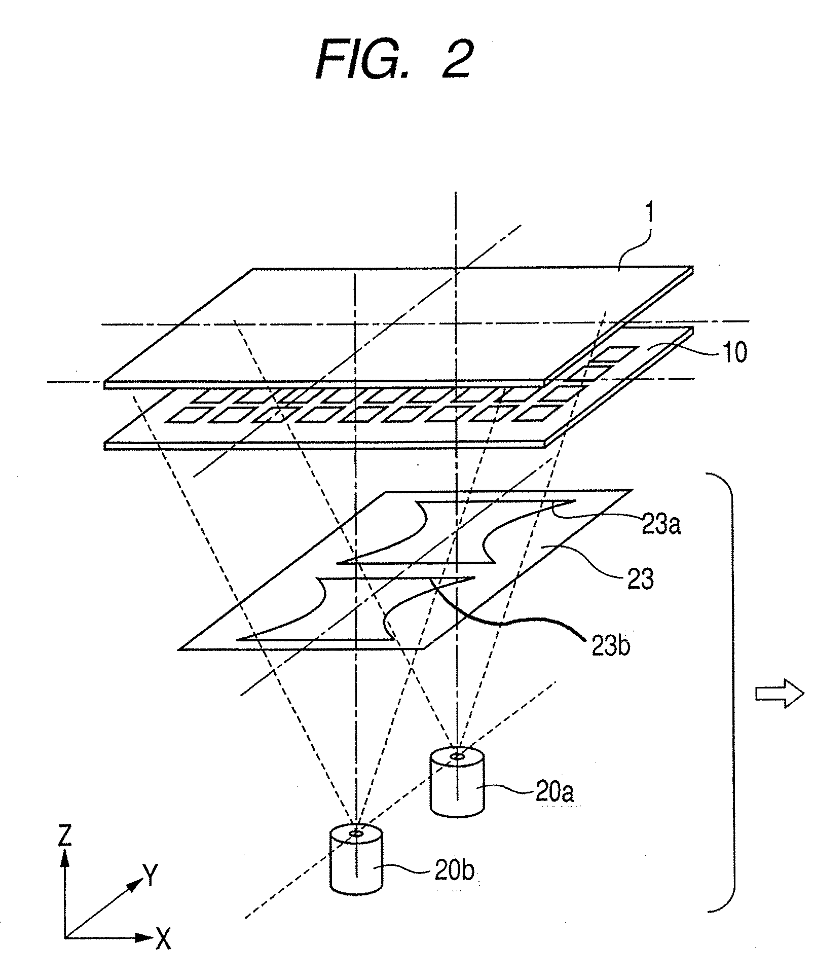
[0075]A substrate of 400 mm×500 mm was used. The substrate was placed such that the length direction thereof was in parallel with the X direction. As illustrated in FIG. 11, end faces of the respective openings 11 in the mask 10 were tapered so as to form an angle φ=about 15°, and with this, the distance between the vapor depositing source and the substrate could be made to be 250 mm.

[0076]The above-described system was used to manufacture an organic light emitting device similarly to the case of the reference example. It is to be noted that, with regard to the vapor deposition rates of the respective organic compounds, the one for a host material of about 12.5 nm / sec was a reference value, and the ones for guest materials were determined according to their respective weight ratios. The velocity of the movement of the vapor depositing source was 20 mm / sec.

[0077]The film thickness distribution of the organic compound layer on the substrate obtained according to the above-described pr...

example 3

[0078]Similarly to the case of Example 2, a substrate of 400 mm×500 mm was used. The substrate was placed such that the length direction thereof was in parallel with the X direction. The distance between the vapor depositing source and the substrate was 250 mm.

[0079]As illustrated in FIG. 12, end faces of the respective openings 11 in the mask 10 were tapered so as to form an angle of about 15°, and the pitch P of the openings in the mask 10 was adjusted so as to be, at the ends of the openings in the film thickness correcting plate 23, shifted by ΔP =10 μm from the centers P0 of pixels on the substrate 1. It is to be noted that there was no shift with regard to the center of the openings in the film thickness correcting plate 23. With this, the width of the openings in the film thickness correcting plate 23 could be made larger. The width Wc of the openings at the center was 170 mm. The rest of the dimensions were determined according to the equations (2).

[0080]The above-described ...


PUM

PropertyMeasurementUnit
Thicknessaaaaaaaaaa
Widthaaaaaaaaaa
Evaporation enthalpyaaaaaaaaaa

Abstract

There is provided a vapor deposition system including a vapor depositing source, holding means for holding a substrate, moving means, and an opening member having an opening, the moving means moving at least one of the substrate, and, the vapor depositing source and the opening member, in one direction in a plane in parallel with a plane including the substrate, and the opening member being disposed between the vapor depositing source and the substrate and having an opening having a width at a center of the opening in a direction of movement which is smaller than that at ends the opening. In the system, the plurality of vapor depositing sources are arranged along a direction in a plane, which is a direction intersecting the direction of movement, and the opening member has a plurality of openings each independently disposed so as to correspond to each of the plurality of vapor depositing sources.

Description

BACKGROUND OF THE INVENTION[0001]1. Field of the Invention[0002]The present invention relates to a vapor deposition system and a vapor deposition method for an organic compound for forming an organic compound layer of an organic light emitting device or the like.[0003]2. Description of the Related Art[0004]FIGS. 13A to 13D illustrate a typical method of manufacturing an organic light emitting device (organic EL) First, a conductive film of high reflectivity is formed on a substrate 101 such as a glass substrate. By patterning the conductive film in a predetermined shape, an anode electrode 102 is formed. Then, a device separating film 103 formed of a highly insulating material is formed so as to surround a pixel 101a on the anode electrode 102. With this, adjacent pixels 101a are partitioned by the device separating film 103. Next, a hole transporting layer 104, an organic light emitting layer 105, an electron transporting layer 106, and an electron injecting layer 107 are formed in...

Claims


Application Information

Patent Timeline
IPC IPC(8): H01L21/31
CPCC23C14/044H01L51/0011C23C14/12H10K71/166H05B33/10
Inventor UKIGAYA, NOBUTAKA
Owner CANON KK
Why Eureka
Try Eureka