Electromagnetic wave shielding film and method for producing the same

a technology film, applied in the field of electromagnetic wave shielding film, can solve the problems of long plating time, low productivity, and inability to avoid image visibility reduction, and achieve the effects of avoiding image visibility reduction, excellent electromagnetic wave shielding properties, and not impairing the visibility of an image displayed

Inactive Publication Date: 2007-08-09
DAI NIPPON PRINTING CO LTD
View PDF4 Cites 12 Cited by
  • Summary
  • Abstract
  • Description
  • Claims
  • Application Information

AI Technical Summary

Benefits of technology

[0023] The present invention provides an electromagnetic wave shielding sheet that has moderate transparency, that is excellent in electromagnetic wave shielding properties and non-recognizability of its mesh, that does not impair the visibility of an image displayed on a display, and that does not undergo deterioration of electromagnetic wave shielding properties by the oxidation of a metal layer.
[0024] The present invention provides an electromagnetic wave shielding sheet that has moderate transpar...

Problems solved by technology

However, this method is disadvantageous in that, since the metal layer face on the transparent substrate side cannot be blackened, it is impossible to avoid lowering of image visibility that is caused by extraneous light such as sunlight that is incident on and is reflected from the metal mesh.
Further, in the production process, if electrically conductive ink is used, it takes a longer time for plating because the electrical resistance of the electrically conductive ink is high, and productivity is therefore low.
Besides, this method...

Method used


Image

  • Electromagnetic wave shielding film and method for producing the same
  • Electromagnetic wave shielding film and method for producing the same
  • Electromagnetic wave shielding film and method for producing the same

Examples


modified embodiments

(Modified Embodiments)

[0070] The present invention encompasses the following modifications.

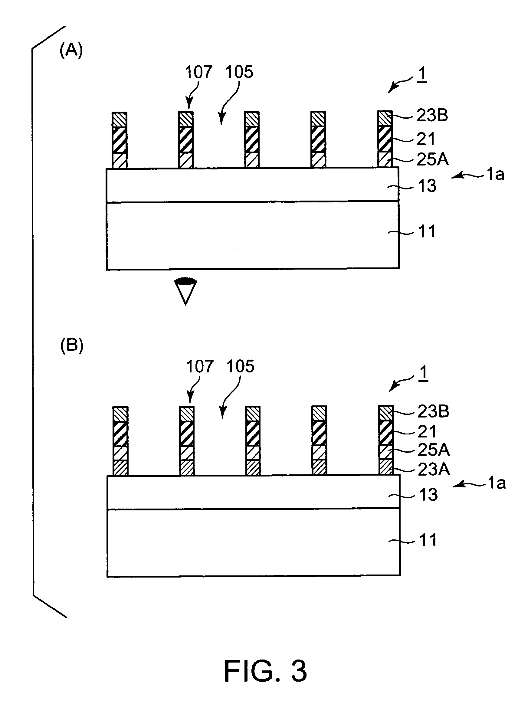
[0071] (1) Although a method of lamination using an adhesive has been employed to laminate the transparent substrate 11 and the [anticorrosive layer 23A / first blackening layer 25A / metal layer 21] to form the laminate 1a, it is not necessary to use the adhesive. For example, after making the surface of the transparent substrate 11 electrically conductive, the first blackening layer 25A and the metal layer 21 may be formed on this surface by a conventional electroless plating or electroplating process.

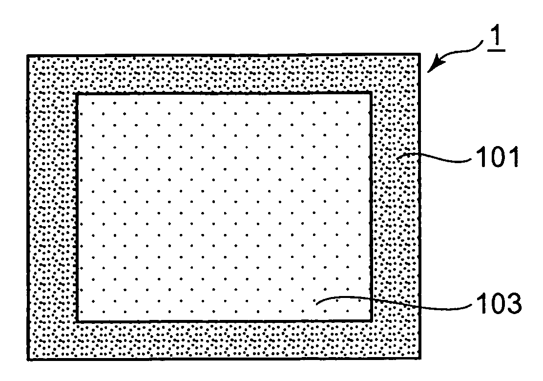
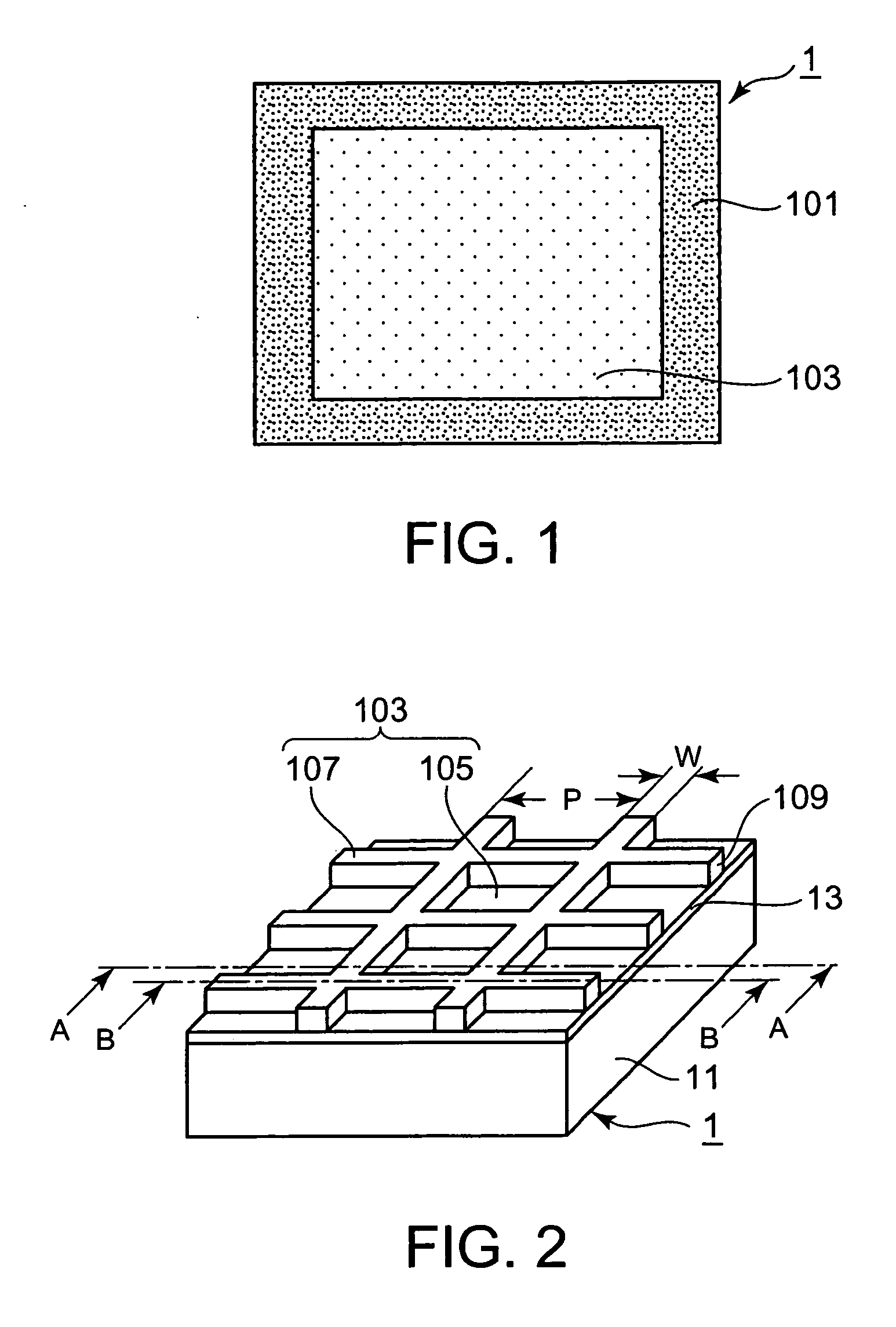
[0072] (2) After obtaining such an electromagnetic wave shielding sheet 1 as is shown in FIG. 3 or 4, the surface of the mesh part 103 that is rough (due to the irregularities brought about by the line parts 107 and the openings 105) may be smoothened by filling the openings 105 with a transparent resin. By doing so, air bubbles never remain in the openings 105 when the mesh part of the electroma...

example 1

[0074] Electrolytic copper foil with a thickness of 10 μm was used as the metal layer 21. Copper-cobalt alloy particles (mean particle diameter: 0.3 μm) were cathodically electrodeposited on one surface of the metal layer 21, thereby conducting blackening treatment to form a first blackening layer 25A.

[0075] Subsequently, the other surface, on the side opposite to the first blackening layer 25A side, of the metal layer 21 was subjected to zinc plating and to chromate treatment, whereby a second anticorrosive layer 23 containing zinc and chromium was formed on this surface of the metal layer 21.

[0076] The combination of the metal layer 21, the second anticorrosive layer 23B, and the first blackening layer 25A was laminated to a transparent substrate 11 made of a biaxially oriented 100-μm thick PET film A4300 (trademark of a polyethylene terephthalate film, manufactured by Toyobo Co., Ltd., Japan) with an adhesive layer 13 of a two-part curing urethane adhesive, and this laminate wa...

example 2

[0079] An electromagnetic wave shielding sheet was obtained in the same manner as in Example 1, except that, in the anticorrosive-layer-forming step, both sides of the metal layer 21 were subjected to anticorrosive treatment to form a [first anticorrosive layer 23A / first blackening layer 25A / metal layer 21 / second anticorrosive layer 23B].


PUM

PropertyMeasurementUnit
Currentaaaaaaaaaa
Currentaaaaaaaaaa
Digital informationaaaaaaaaaa

Abstract

An electromagnetic wave shielding sheet 1 comprises a transparent substrate 11, and a first anticorrosive layer 23A, a first blackening layer 25A, a metal layer 21, and a second anticorrosive layer 23B that are successively formed on the transparent substrate 11 through an adhesive layer 13. A second blackening layer 25B is formed so that it fully covers the side faces of the first anticorrosive layer 23A, the first blackening layer 25A, the metal layer 21, and the second anticorrosive layer 23B, as well as the front face of the second anticorrosive layer 23B. At least either of the first anticorrosive layer 23A and the second anticorrosive layer 23B contains one or more metals selected from nickel, chromium, and silicon, and also zinc and/or tin when it is initially formed, and the zinc and/or tin is removed from the first anticorrosive layer 23A and/or the second anticorrosive layer 23B in an intermediate steps.

Description

FIELD OF THE INVENTION [0001] The present invention relates to an electromagnetic wave shielding sheet for preventing EMI (electromagnetic (wave) interference) that is caused by electromagnetic waves generated by such displays as cathode ray tubes (hereinafter also referred to as CRTs) and plasma display panels (hereinafter also referred to as PDPs), and, more particularly, to an electromagnetic wave shielding sheet that does not impair the visibility of an image displayed on a display and that can be produced in a small number of steps, and to a method for producing the electromagnetic wave shielding sheet. [0002] In this Specification, “ratio”, “part”, “%”, and the like that indicate proportions are on a weight basis unless otherwise specified, and the symbol “ / ” denotes that layers enumerated together with this symbol are integrally laminated. “EMI”, “NIR”, and “PET” designate “electromagnetic (wave) interference”, “near infrared rays”, and “polyethylene terephthalate”, respectiv...

Claims


Application Information

Patent Timeline
IPC IPC(8): H01B11/06C23C28/00C25D5/02C25D7/00H05K9/00
CPCC25D3/562C25D5/02H05K9/0096C25D7/0614C25D15/00C25D5/10C25D5/611C25D5/627H05K9/00
Inventor NAITO, NOBUOARAKAWA, FUMIHIROMASAKI, TADAHIRO
Owner DAI NIPPON PRINTING CO LTD
Why Eureka
Try Eureka