Apparatus and method for wafer surface defect inspection

a technology of surface defect and apparatus, applied in the field of wafer surface defect inspection, can solve the problems of inadequately defining a method inadequately defining a method for minimizing, and the patent documents 1 to 5 do not adequately define a method for correcting displacement and dimensions, etc., to achieve accurate identification, accurate collation of vertical irradiation results, and high precision

Inactive Publication Date: 2007-08-09
HITACHI HIGH-TECH CORP
View PDF5 Cites 66 Cited by
  • Summary
  • Abstract
  • Description
  • Claims
  • Application Information

AI Technical Summary

Benefits of technology

[0009] The present invention has been made to solve the above problems and provides a wafer surface defect inspection apparatus and method for determining, for instance, the position coordinates of extremely small foreign matter and other defects on the wafer surface with high precision, accurately collating vertical irradiation results with oblique irradiation results, and accurately identifying the types (categories) of foreign matter and other defects while minimizing the detection sensitivity and detected position coordinate variations among apparatuses.

Problems solved by technology

However, Patent Documents 1 to 5 do not adequately define a method for correcting the displacement and dimensions of a vertical irradiation beam spot and oblique irradiation beam spot on the surface of a wafer with high precision and accurately detecting, for instance, the position coordinates of extremely small foreign matter or other defects on the surface of the wafer without being affected by the film thickness variation and film quality of the wafer surface even when the wafer surface is warped, undulated, or otherwise deformed.
Further, the patent documents do not adequately define a method for minimizing the detection sensitivity and detected position coordinate variations among apparatuses.

Method used


Image

  • Apparatus and method for wafer surface defect inspection
  • Apparatus and method for wafer surface defect inspection
  • Apparatus and method for wafer surface defect inspection

Examples


first embodiment

[0049] First of all, a first embodiment of the wafer surface defect inspection apparatus according to the present invention will be described with reference to FIGS. 1 to 9.

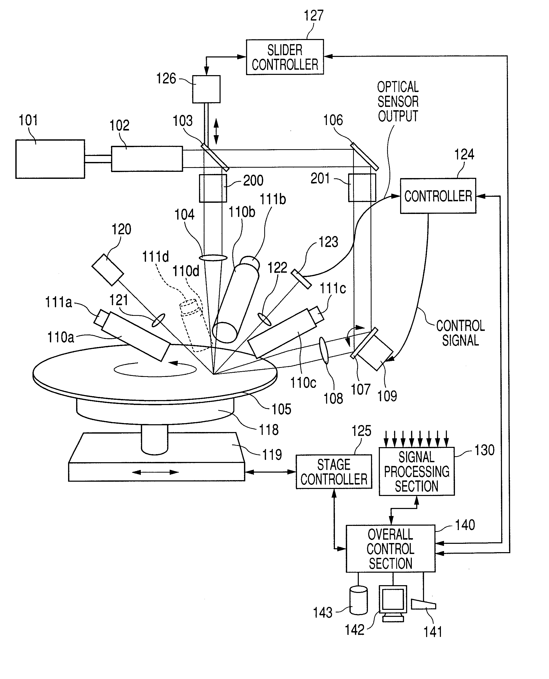
[0050]FIG. 1 is a diagram illustrating the wafer surface defect inspection apparatus according to the first embodiment of the present invention. It is preferred that, for example, a laser light source for emitting UV (ultraviolet) or DUV (deep ultraviolet) light to obtain high-intensity scattered light from extremely small foreign matter and other defects be used as a first light source 101 in order to detect extremely small foreign matter and other defects on a semiconductor wafer 105. More specifically, an argon laser, harmonic YAG laser, excimer laser, or the like should be used. The light emitted from the first light source 101 travels through a beam expander 102, bounces off a controllable mirror 103, which can be controlled by a uniaxial slider 126 such as an air cylinder or electric cylinder, passes throu...

second embodiment

[0078] A second embodiment of the present invention will now be described with reference to FIG. 12. The second embodiment differs from the first embodiment in that the former includes observation optics 204-207, which observe the position and shape (illumination distribution included) of a beam spot image formed on the wafer; a beam correction optics 202, which corrects the tilt (gradient: emission direction) and shift (displacement: emission position) of a beam emitted from the first light source 101 relative to the optical axis; a controller 208, which controls the beam correction optics 202 in accordance with the position and shape of the beam spot image observed by the observation optics 204-207; and a controller 209, which controls a zoom type beam expander (beam diameter enlargement optics) 203 in accordance with the position and shape of the beam spot image observed by the observation optics 204-207. It should be noted that the slider controller 127 is not shown in FIG. 12. ...

third embodiment

[0095] A third embodiment of the present invention will now be described with reference to FIG. 18. The third embodiment differs from the second embodiment in that the former includes magnification adjustment / beam shaping optics 220, 221 and a beam spot profile correction element 901. It should be noted that the slider controller 127 is not shown in FIG. 18 either.

[0096] The beam emitted from the first light source 101 falls on the beam correction optics 202, which corrects the tilt and shift relative to the optical axis. The beam emitted from the beam correction optics 202 travels through the profile correction element 901 and falls on the zoom type beam expander 203. The beam emitted from the zoom type beam expander 203 bounces off the controllable mirror 103, travels through the magnification adjustment / beam shaping optics 220, beam splitter 204, and vertical irradiation condenser lens 104, and falls on the wafer 105 from a substantially vertical direction to form a vertical irr...


PUM

PropertyMeasurementUnit
wavelengthaaaaaaaaaa
deflection angleaaaaaaaaaa
angleaaaaaaaaaa

Abstract

A beam emitted from a first light source is shed on the surface of a rotating wafer to form a beam spot. Scattered light arising from foreign matter and other defects on the surface of the wafer is detected in a plurality of directions and output in the form of a signal. Vertical movement of the wafer surface is detected by using white light or broadband light from a second light source. The position of the beam spot on the wafer surface is corrected in accordance with the information on the detected vertical movement for the purpose of minimizing a coordinate error that may arise from the vertical movement of the wafer surface. Further, the emission direction and emission position of light generated from the first light source are corrected to minimize a coordinate error that may arise from variations of the first light source. These corrections are made to enhance the accuracy of the coordinates of detected foreign matter and other defects. Moreover, the illumination beam spot diameter is corrected to prevent the detection sensitivity and foreign matter coordinate detection error from varying from one apparatus to another.

Description

BACKGROUND OF THE INVENTION [0001] The present invention relates to a wafer surface defect inspection apparatus and method for inspecting the surface of a bare wafer without a semiconductor pattern, a filmed wafer without a semiconductor pattern, or a disk for foreign matter and other defects. [0002] Conventionally known technologies for inspecting the surface of a bare wafer without a semiconductor pattern, a filmed wafer without a semiconductor pattern, and the like for foreign matter and other defects are disclosed, for instance, by U.S. Pat. No. 6,201,601 (Patent Document 1), Japanese Patent JP-A No. 153549 / 1999 (Patent Document 2), Japanese Patent JP-A No. 242012 / 1994 (Patent Document 3), Japanese Patent JP-A No. 255278 / 2001 (Patent Document 4), and U.S. Pat. No. 6,922,236 (Patent Document 5). [0003] The technology described in Patent Document 1 uses a laser as a light source, causes an illumination optics to irradiate a wafer with a vertical beam and an inclined beam, collects...

Claims


Application Information

Patent Timeline
Patent Type & Authority Applications(United States)
IPC IPC(8): G01N21/88
CPCG01N21/8851G01N2021/8861G01N2021/4711G01N21/9501
Inventor MANABE, YUJIJINGU, TAKAHIRO
Owner HITACHI HIGH-TECH CORP
Why Eureka
Try Eureka