

Distributed feedback semiconductor laser
- Summary
- Abstract
- Description
- Claims
- Application Information
AI Technical Summary
Benefits of technology
Problems solved by technology
Method used
Image

Examples
Embodiment Construction
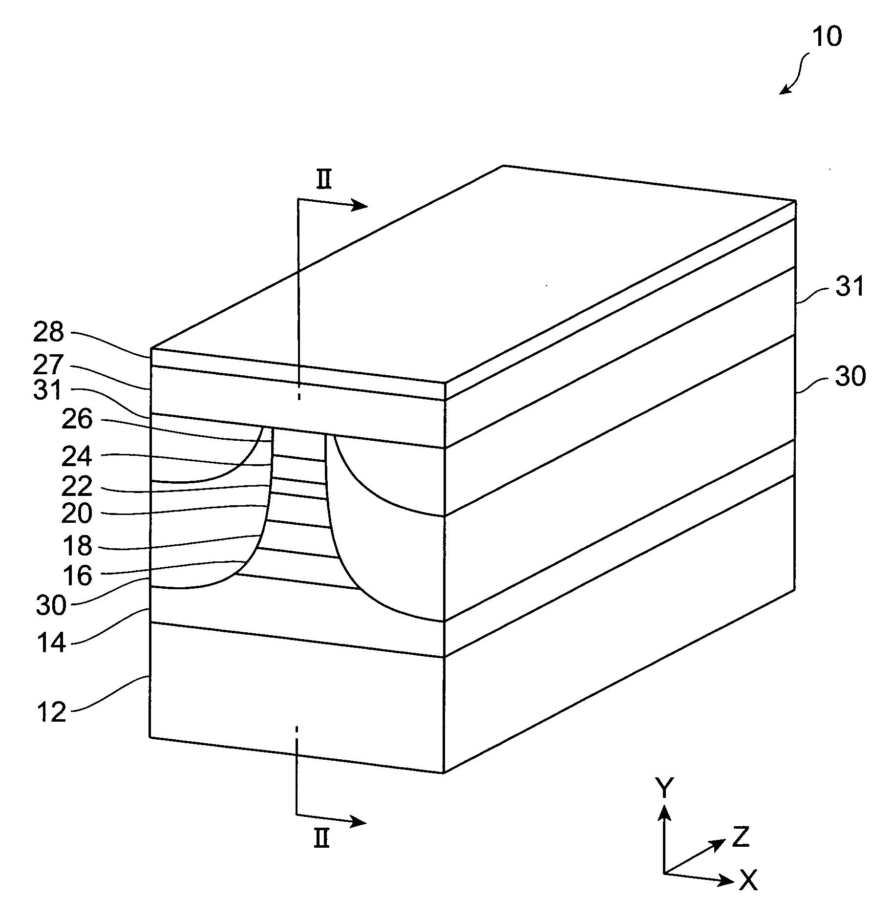
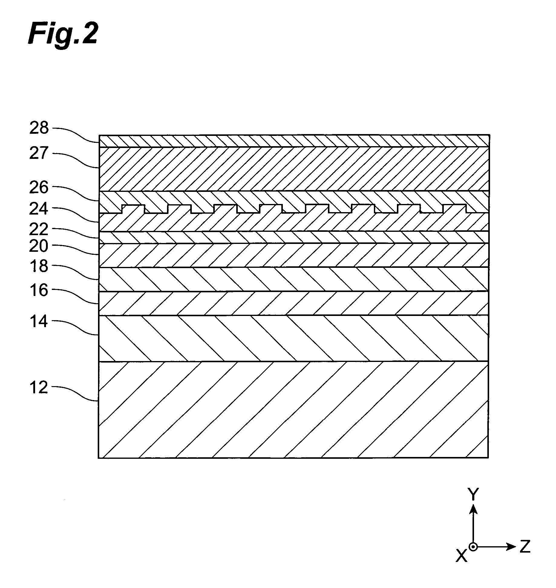
[0019] Referring to the accompanying drawings, embodiments of the present invention will be explained. When possible, parts identical to each other will be referred to with symbols identical to each other.
[0020]FIG. 1 is a diagrammatic perspective view showing the structure of a distributed feedback semiconductor laser according to the present embodiment. FIG. 2 is a view showing the cross section taken along the II-II line shown in FIG. 1. Referring to FIGS. 1 and 2, a number of semiconductor layers are provided on an n-type InP substrate 12 in a distributed feedback semiconductor laser 11. A first n-type Inp cladding layer 14 is provided on the n-type InP substrate 12, a first optical guide AlGaInAs layer 16 is provided on the first n-type InP cladding layer 14, an AlGaInAs active layer 18 is provided on the first optical guide AlGaInAs layer 16, a second optical guide AlGaInAs layer 20 is provided on the active layer 18, an InP semiconductor layer 22 is provided on the second op...
PUM
 Abstract
Description
Claims
Application Information