Double-side polishing carrier and fabrication method thereof

a polishing carrier and fabrication method technology, applied in the direction of work carriers, electrical devices, decorative arts, etc., can solve the problems of high production cost, high production cost, and high production cost of base materials, so as to facilitate the fabrication of base materials and resin inserts, the effect of increasing production cost and improving manufacturing efficiency

Inactive Publication Date: 2007-08-09
SUMCO TECHXIV
View PDF8 Cites 25 Cited by
  • Summary
  • Abstract
  • Description
  • Claims
  • Application Information

AI Technical Summary

Benefits of technology

[0056] As shown in FIG. 7, to fix the resin insert 15 to the base material 10a of the double-side polishing carrier 10, it is generally necessary to dispose a peculiar shape such as the wedges 10c or the wedges 15b on the inner wall 11a of the holding openings 11 or the outer side wall 15a of the resin insert 15 formed in the base material 10a. To form such a shape, it is necessary to increase the fabrication works of the base material 10a and the resin insert 15, but there are problems that manufacturing efficiency of the base material 10a and the resin insert 15 lowers, and the production cost increases.
[0057] As shown in FIG. 8, the seventh aspect has the base material 10a and a resin 20 coated with a coating layer 21 of a material having hardness higher than that of the base material 10a. In other words, the coating layer 21 covers a bonded portion 22 between the base material 10a and the resin insert 20. The resin insert 20 is fixed to the base material 10a with the coating layer 21. Therefore, the same effect as that provided by the first aspect can be obtained according to the seventh aspect, and the fabrication of the base material and the resin insert is facilitated because the base material and the resin insert do not require the wedges. Thus, the manufacturing efficiency of the base material and the resin insert is improved, and the production cost is reduced. And, damage to the silicon wafer is decreased because the silicon wafer is held by the resin insert.

Problems solved by technology

But, the double-side polishing carriers 10 made of stainless steel have low thickness accuracy and are variable in thickness.
Therefore, the individual silicon wafers 1 which are finished by the individual double-side polishing carriers 10 have a disadvantage that their flatness is variable.
Besides, there is a problem that the double-side polishing carriers 10 are abraded quickly.
Therefore, there is a problem that the silicon wafers 1 are variable in flatness depending on the progress of the abrasion of the double-side polishing carriers 10, so that they cannot be provided with stable flatness.
There is also a problem that where the double-side polishing carriers 10 are worn, metal powder produced as a result causes metal contamination of the silicon wafers 1.
And, there is another problem that where the double-side polishing carriers 10 are worn, the metal powder produced as a result causes scratches on the surfaces of the silicon wafers 1.
Because the double-side polishing carriers 10 are worn quickly, a replacement cycle of the double-side polishing carriers 10 is short, resulting in high cost.
Therefore, the replacement cycle of the polishing cloth 103, 104 becomes short, resulting in high cost.
Therefore, the edge surfaces 1c of the silicon wafers 1 might be damaged.

Method used


Image

  • Double-side polishing carrier and fabrication method thereof
  • Double-side polishing carrier and fabrication method thereof
  • Double-side polishing carrier and fabrication method thereof

Examples


Embodiment Construction

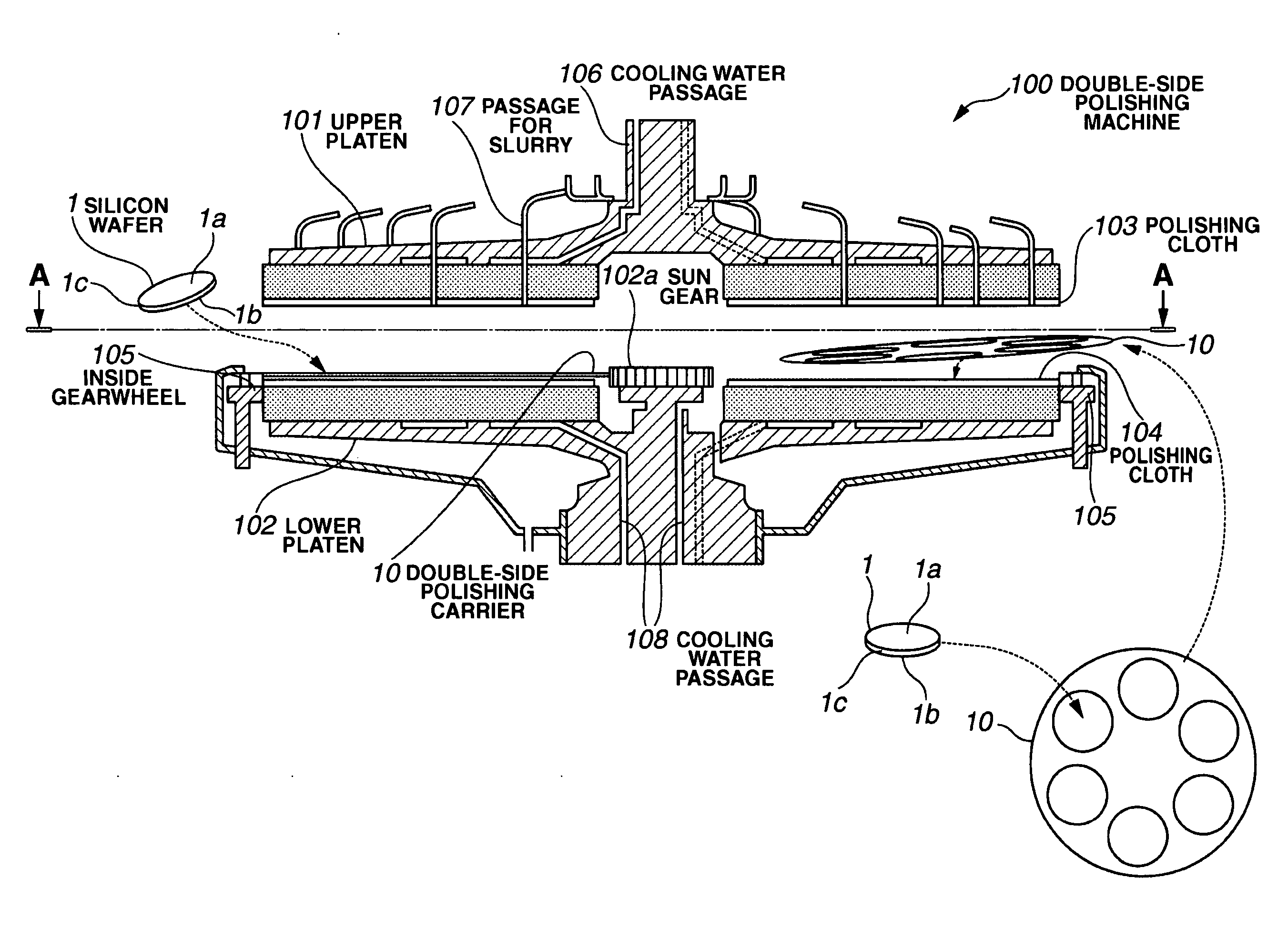
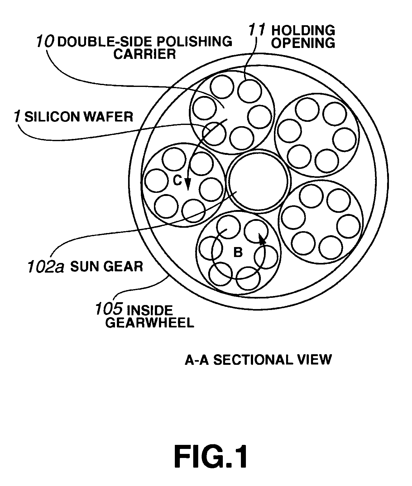
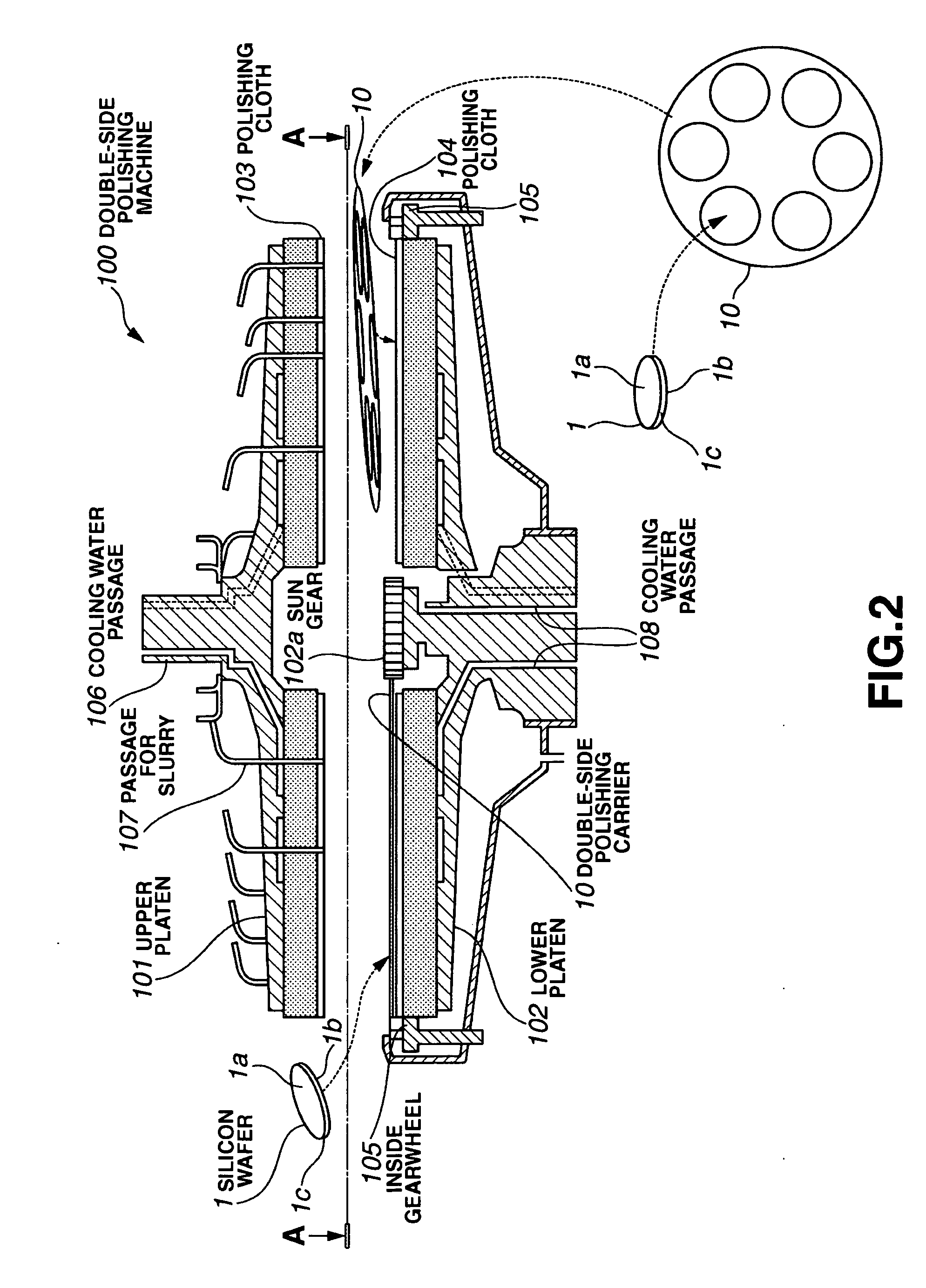
[0058] A double-side polishing carrier according to the present invention will be described with reference to the drawings. It is assumed in the embodiments that silicon wafers are polished by means of a double-side polishing carrier. It should be understood that “polishing” used through the specification includes a meaning of lapping, and the “double-side polishing carrier” is used as a double-side polishing carrier to be used for a double-side polishing machine in the polishing step, and also means a carrier used for a double-side polishing machine (both-side lapping apparatus) in the lapping step.

[0059] The double-side polishing carrier of the invention can also be used to polish not only the silicon wafers but also other semiconductor wafers of gallium arsenide and the like.

[0060]FIG. 2 is a side view of the double-side polishing machine 100. FIG. 1 is a top view taken in the direction of arrows A of the double-side polishing machine 100 of FIG. 2, showing a positional relatio...


PUM

PropertyMeasurementUnit
thicknessaaaaaaaaaa
roughnessaaaaaaaaaa
friction coefficientaaaaaaaaaa

Abstract

The carrier (10) for double-side polishing has a base material 10a the material of which is stainless steel (SUS) , for example, as is before, and the base material 10a is coated with a coating layer 10b of a material having a hardness higher than that of the base material 10a. The coating layer 10b is desirably coated uniformly without variations in thickness and not warped easily, and the material for the coating layer 10b of the double-side polishing carrier 10 is desirably any one selected from diamond-like carbon, a nitride film, a sapphire film and a titanium nitride film. For production of the double-side polishing carrier 10, a double-side polishing carrier 10′ having been used for polishing is prepared first. The used carrier 10′ is coated with the coating layer 10b. The invention can suppress the progress of abrasion of the double-side polishing carrier, and can provide satisfactory thickness accuracy, film thickness distribution accuracy, and surface roughness.

Description

TECHNICAL FIELD [0001] The present invention relates to a double-side polishing carrier used for double-side polishing machines and a fabrication method thereof. BACKGROUND ART [0002] Silicon wafers are fabricated through individual steps including a lapping step and a polishing step. [0003] In the polishing step, the silicon wafer is simultaneously polished on both sides by means of a double-side polishing machine. In the lapping step, the both sides of the silicon wafer are simultaneously lapped by means of a both-side lapping apparatus. The outline of the apparatus will be described below with reference to the double-side polishing machine as a representative. [0004]FIG. 2 is a side view of a double-side polishing machine 100. FIG. 1 is a top view taken in the direction of arrows A of the double-side polishing machine 100 of FIG. 2, showing a positional relationship among double-side polishing carriers 10, silicon wafers 1 and a lower platen 102. [0005] The double-side polishing ...

Claims


Application Information

Patent Timeline
Patent Type & Authority Applications(United States)
IPC IPC(8): C03C15/00H01L21/306B44C1/22H01L21/302B24B37/28
CPCB24B37/28
Inventor YAMASHITA, KENJIOONO, YUKIOSUGIMOTO, YUUJI
Owner SUMCO TECHXIV
Why Eureka
Try Eureka