Printed circuit board, method of producing the same, and electronic unit

a technology of printed circuit boards and printed circuits, applied in the direction of resist details, second resist masks, semiconductor/solid-state device details, etc., can solve the problems of inability to manufacture resin, inability to reduce the thickness of circuits, and inability to reduce circuit thickness

Inactive Publication Date: 2007-08-16
RICOH KK
View PDF7 Cites 20 Cited by
  • Summary
  • Abstract
  • Description
  • Claims
  • Application Information

AI Technical Summary

Benefits of technology

[0030] According to the present invention, because an insulating material layer may be formed on the printed circuit board and may at least have an opening in a region where the electrode is formed, and the resin-outflow-prevention dam may be formed from the insulating material, the resin-outflow-prevention dam may be formed by removing an unnecessary portion of the insulating material layer. Hence, additional steps are not needed to form the resin-outflow-prevention dam, and this makes it easy to fabricate the resin-outflow-prevention dam.

Problems solved by technology

When sealing elements on the printed circuit board by potting, if the viscosity of a potting resin is high, the resin can hardly spread, so that the height of the resin after curing is large, and this makes it difficult to reduce the thickness of the circuit and therefore not suitable for fabricating compact circuit boards.
On the other hand, if the viscosity of the potting resin is low, the resin cannot be too high, but it spreads easily and covers an excessively broad region.
However, because the water-repellent effect of silicon is very strong, the potting resin 50 cannot be applied to the end of the sealing region.
Similarly, when the viscosity of the resin-outflow-prevention dam 44 is high, the fabrication process becomes complicated, too.
However, such a resin-outflow-prevention dam 44 has a weak adhesive force with the epoxy resin on the printed circuit board, and low water-resistance; thus, the process of forming the sealing frame has to be fixed.
When the resin-outflow-prevention dam 44 is formed from a solder resist, as in the reference 3, usually the thickness of the resist is about 20 μm, which is very thin, and thus, this method is not applicable to situations requiring a certain height for potting.

Method used


Image

  • Printed circuit board, method of producing the same, and electronic unit
  • Printed circuit board, method of producing the same, and electronic unit
  • Printed circuit board, method of producing the same, and electronic unit

Examples


first embodiment

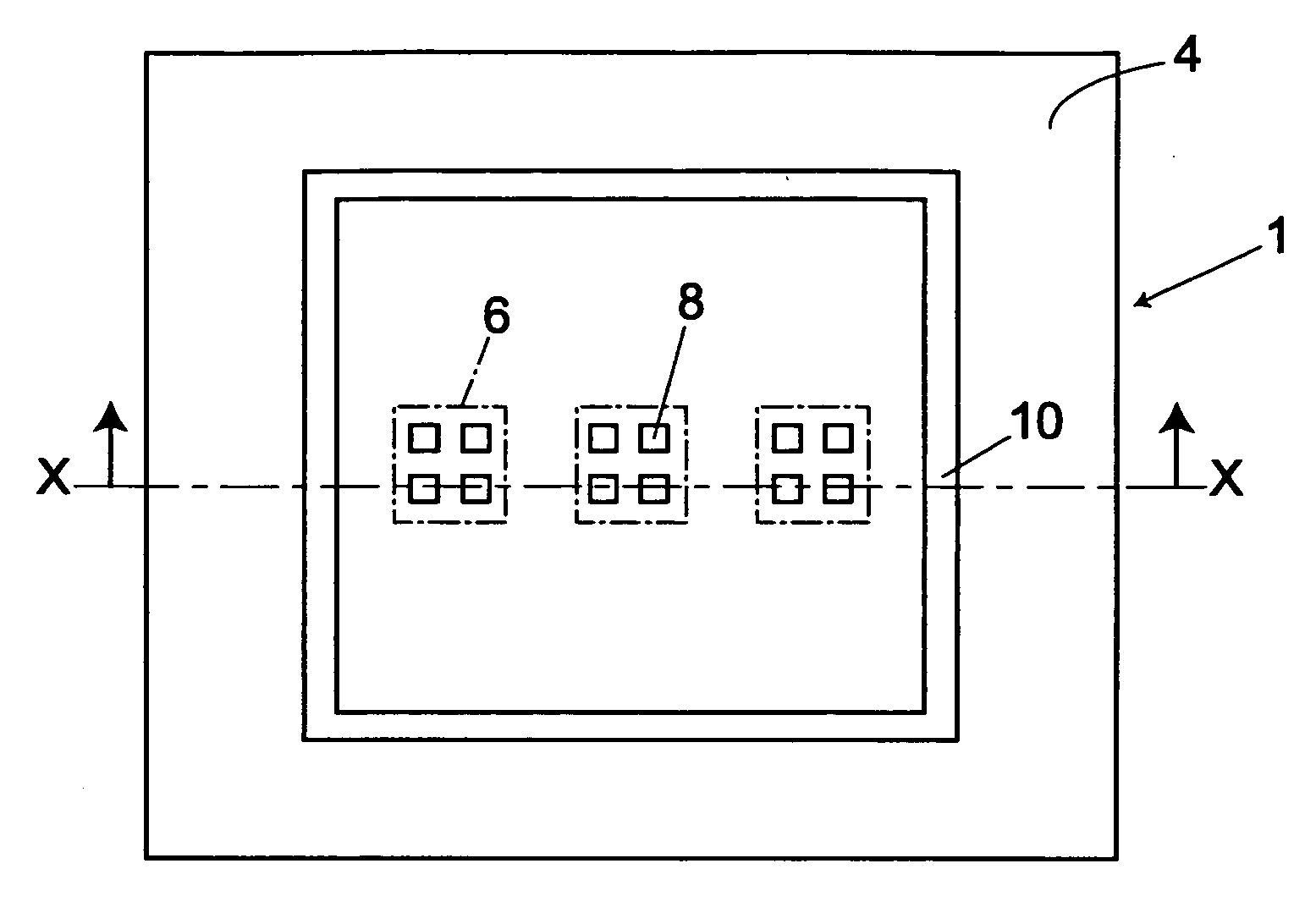
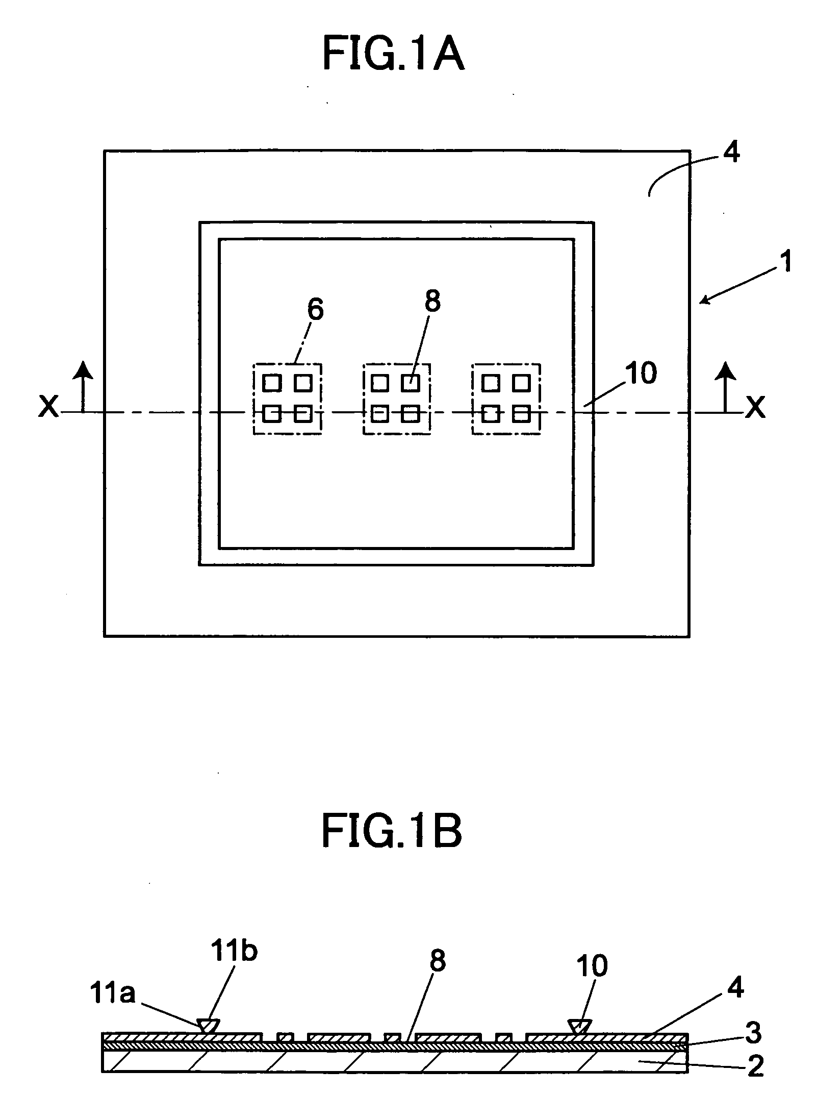
[0049]FIG. 1A is a plan view of a printed circuit board according to a first embodiment of the present invention.

[0050]FIG. 1B is a cross-sectional view of the printed circuit board in FIG. 1A along an X-X line in FIG. 1A.

[0051] As illustrated in FIG. 1A, in a printed circuit board 1, a conductive pattern 3 is formed on an insulating substrate 2 by patterning a metal layer on the insulating substrate 2, and a solder resist 4 is formed on the conductive pattern 3 as an insulating material layer. The solder resist 4 has functions of preventing degradation of the printed circuit board 1 caused by oxidation of the conductive pattern 3, and preventing a short between the solder applied when mounting electronic parts and electrodes nearby or the conductive pattern 3. For example, the solder resist 4 is made from PSR-4000 G30, manufactured by Taiyo Ink Co.

[0052] In the printed circuit board 1, for example, three mounting areas 6 are provided in the printed circuit board 1 for mounting t...

second embodiment

[0078]FIG. 4A is a plan view of a printed circuit board according to a second embodiment of the present invention.

[0079]FIG. 4B is a cross-sectional view of the printed circuit board in FIG. 4A along a Y-Y line in FIG. 4A.

[0080] As illustrated in FIG. 4A, in a printed circuit board 20, a conductive pattern 23 is formed on an insulating substrate 22, and a solder resist 24 is formed in the peripheral region of mounting areas 26, where electronic parts (such as, semiconductor devices) are to be mounted. The solder resist 24 has functions of preventing degradation of the printed circuit board 20 caused by oxidation of the conductive pattern 23, and preventing a short between the solder applied when mounting the electronic parts and electrodes nearby or the conductive pattern 3.

[0081] In the printed circuit board 20, for example, three mounting areas 26 are provided, and three groups of electrodes 28, each of which groups includes four electrodes 28, are formed in the three mounting ...

third embodiment

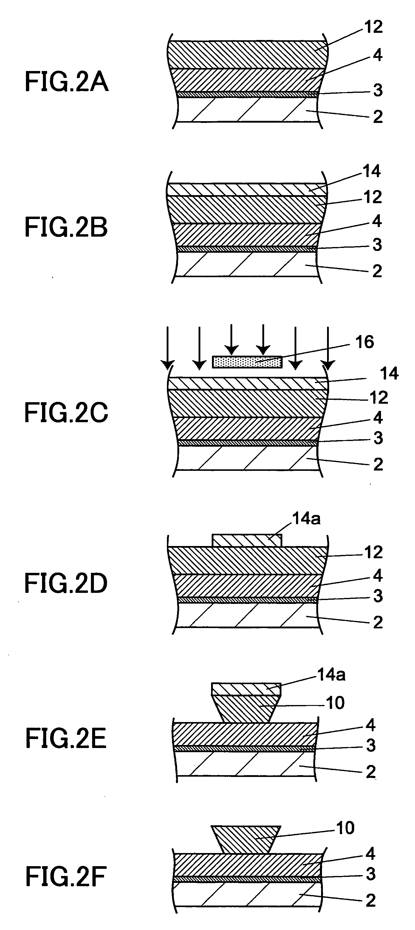
[0090]FIG. 5A is a cross-sectional view of an electronic unit according to a third embodiment of the present invention.

[0091]FIG. 5B is an enlarged cross-sectional view of a portion of the electronic unit indicated by a dashed circle in FIG. 5A.

[0092] In the following descriptions, the same reference numbers are assigned to the same elements as those described in the previous embodiments, and overlapping descriptions are omitted.

[0093] In FIG. 5A, three electronic parts 32 are mounted on the mounting areas 26 of the printed circuit board 1. For example, the electronic parts 32 are flip chip semiconductor devices, in each of which connection terminals (not illustrated) are provided on the back surface. The connection terminals on the back surface of each of the electronic parts 32 are electrically connected to the mounting electrodes 8 on the printed circuit board 1 through solder 34, and the electronic parts 32 are electrically connected to external electric devices through the c...


PUM


Abstract

A printed circuit board is disclosed that is able to prevent outflow of a potting resin out of a sealing region. The printed circuit board includes a conductive pattern formed on an insulating substrate, an electrode for connecting an electronic part to the conductive pattern, and a stripe-like resin-outflow-prevention dam arranged in a periphery of a resin-sealing region covering the electronic part. An outer side surface and an upper surface of the resin-outflow-prevention dam subtend an acute angle.

Description

BACKGROUND OF THE INVENTION [0001] 1. Field of the Invention [0002] The present invention relates to a printed circuit board including a conductive pattern formed on the surface of an insulating substrate, a mounting electrode for connecting an electronic part to the conductive pattern, and a stripe-like resin-outflow-prevention dam provided in a periphery of a resin sealing region covering the area where the electronic part is mounted to prevent outflow of resin, a method of forming the resin-outflow-prevention dam, and an electronic unit including the printed circuit board. [0003] 2. Description of the Related Art [0004] In an electronic unit including elements such as semiconductor chips, flip chips, or resistors mounted on a printed circuit board, in order to protect these elements, they are sealed by using resin. For example, there is a simple method of sealing the elements by potting, in which liquid resin is potted onto a circuit portion for sealing. [0005] When sealing eleme...

Claims


Application Information

Patent Timeline
Patent Type & Authority Applications(United States)
IPC IPC(8): H05K1/00
CPCH01L23/24H05K3/284H05K2203/0585H05K2203/0588H05K2203/0594H01L2224/48091H01L2924/3025H01L2224/73265H01L2924/00014H01L2924/00
Inventor HIGASHIGUCHI, MASAHIROTAN, KUNIHIRO
Owner RICOH KK
Why Eureka
Try Eureka