Array substrate of liquid crystal display and fabricating method thereof

a liquid crystal display and substrate technology, applied in non-linear optics, instruments, optics, etc., can solve the problems of decreasing the aperture ratio of the lcd, increasing the area of the storage electrode, etc., to reduce flicker, reduce the number of fabrication steps, and increase the electrostatic capacitance of the storage capacitor.

Inactive Publication Date: 2007-08-16
LG DISPLAY CO LTD
View PDF10 Cites 29 Cited by
  • Summary
  • Abstract
  • Description
  • Claims
  • Application Information

AI Technical Summary

Benefits of technology

[0024] Accordingly, it is an object of the present invention to provide a liquid crystal display (LCD) and a fabricating method thereof that is capable of increasing the electrostatic capacitance of a storage capacitor without decreasing the aperture ratio of the LCD to reduce flickers and lessen the number of fabrication steps.

Problems solved by technology

However, an increase of the area of the storage electrode decreases the aperture ratio of the LCD.

Method used


Image

  • Array substrate of liquid crystal display and fabricating method thereof
  • Array substrate of liquid crystal display and fabricating method thereof
  • Array substrate of liquid crystal display and fabricating method thereof

Examples


Embodiment Construction

[0058] With reference to FIGS. 9 to 26, preferred embodiments of the present invention are explained as follows.

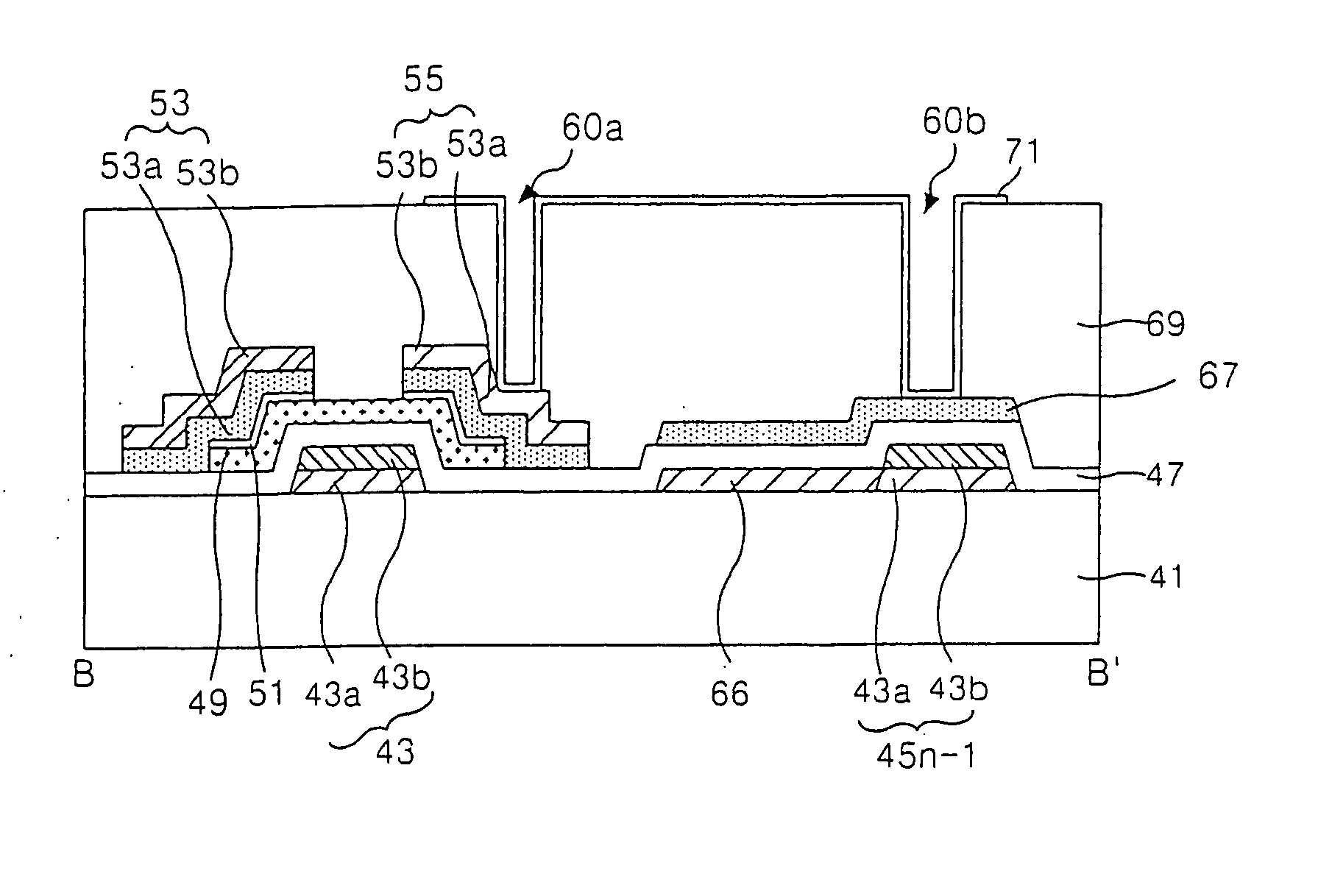
[0059] Referring to FIGS. 9 and 10, a lower substrate 41 of a liquid crystal display according to an embodiment of the present invention includes a TFT 58 located at the intersection of a data line 54 and a gate line 45n, a pixel electrode 71 connected to a drain electrode 55 of the TFT 58, and a storage capacitor 56 located at the overlapping area of the pixel electrode 71 and a previous gate line 45n−1.

[0060] The TFT 58 includes a gate electrode 43 connected to a gate line 45n, a source electrode 53 connected to the data line 54, and a drain electrode 55 connected to the pixel electrode 71 through a first contact hole 60a. The TFT 58 further includes a gate insulating film 47 for insulating the gate electrode 43 from the source and drain electrodes 53 and 55, and semiconductor layers 49 and 51 for defining a channel between the source electrode 53 and the drain electro...


PUM

PropertyMeasurementUnit
thicknessaaaaaaaaaa
capacitanceaaaaaaaaaa

Abstract

An array substrate of a liquid crystal device has a plurality of gate lines, data lines, pixel areas, and thin film transistors, wherein the gate lines are formed from a material of a first and second metal layer, and wherein the first metal layer of the gate line is extended on the pixel area. Also, a display device has first and second gate lines and a data line on a substrate, a thin film transistor, a pixel electrode, a first storage electrodes extending from the second gate line and wherein at least one of the first and second gate lines and the data line includes first and second line layers respectively formed of an oxidized metal later and a metal layer.

Description

CROSS-REFERENCE TO RELATED APPLICATION [0001] The application is a Continuation of co-pending application Ser. No. 10 / 183,683, filed on Jun. 28, 2002, which claims priority to Korean Patent Application No. P2001-40605 filed Jul. 7, 2001, the entire contents of which are hereby incorporated by reference.BACKGROUND OF THE INVENTION [0002] 1. Field of the Invention [0003] This invention relates to an array substrate of a liquid crystal display and a fabricating method thereof, and more particularly to an array substrate of a liquid crystal display and a fabricating method thereof that is capable of increasing the electrostatic capacitance of a storage capacitor without any decrease of an aperture ratio to reduce flickers and to lessen the number of required processes. [0004] 2. Description of the Related Art [0005] Generally, a liquid crystal display LCD controls a light transmittance of a liquid crystal using an electric field to display a picture. To this end, the LCD includes a liqu...

Claims


Application Information

Patent Timeline
Patent Type & Authority Applications(United States)
IPC IPC(8): G02F1/136G02F1/1343G02F1/1362
CPCG02F2001/13629G02F1/136213G02F1/13629G02F1/1343
Inventor HWANG, KWANG JOKIM, WOO HYUNKIM, SE JUNG
Owner LG DISPLAY CO LTD
Why Eureka
Try Eureka