Magnetic sensor and current sensor

a current sensor and magnetic sensor technology, applied in the field of magnetic sensors, can solve the problems of increasing the stability of detection sensitivity and responsibility, the influence of external noise, and the inability to adjust the detection sensitivity, so as to improve the stability of detection sensitivity and responsibility, the uniaxial anisotropy of the free layer can be increased more, and the effect of high precision and stability

Active Publication Date: 2007-08-16
TDK CORPARATION
View PDF8 Cites 79 Cited by
  • Summary
  • Abstract
  • Description
  • Claims
  • Application Information

AI Technical Summary

Benefits of technology

[0015]According to the magnetic sensor of the embodiment of the present invention, a magnetoresistive element is formed by layering in order a free layer having a magnetization direction that varies in accordance with a magnetic field to be detected, an intermediate layer and a pinned layer having the magnetization direction that is pinned to a direction orthogonal to the magnetization direction of the free layer under no external magnetic field; a bias magnetic field is applied to the foregoing magnetoresistive element along the magnetization direction of the free layer under no magnetic field to be detected, using a bias applying means. Accordingly, uniaxial anisotropy of the free layer can be increased more. As a result, the magnetic field to be detected can, be detected with high precision and stability without depending on the configuration of the magnetoresistive element, which is advantageous to miniaturization.
[0016]According to the first and the second current sensors of the embodiment of the present invention, a magnetoresistive element is formed by layering in order a free layer having a magnetization direction that varies in accordance with a magnetic field generated in accordance with current to be detected, an intermediate layer and a pinned layer having a magnetization direction that is pinned to a direction orthogonal to the magnetization direction of the free layer under no foregoing magnetic field; a bias magnetic field is applied to the foregoing magnetoresistive element along the magnetization direction of the free layer under no foregoing magnetic field, using the bias applying means. Accordingly, uniaxial anisotropy of the free layer can be increased more. As a result, magnetic field to be detected can be detected with high precision and stability without depending on the configuration of the magnetoresistive elements, which is advantageous to miniaturization. In particular, according to the second current sensor, the first and the second magnetoresistive elements are arranged along the conductor so as to develop an opposite-directional variation each other in accordance with the current magnetic field, so that the current to be detected can be detected based on a difference of voltage drops respectively produced when constant currents of a common value are supplied to the first and the second magnetoresistive elements. Accordingly, the current sensor allows the current magnetic field, which is generated by the current to be detected, to be detected with high precision and stability while realizing a compact configuration.

Problems solved by technology

However, in association with the miniaturization in dimension, the magnetic sensors and the current sensors, even if using the GMR elements, are susceptible to influences of an external noise (such as unnecessary magnetic field, etc.).
Therefore, improvement in stability in the detection sensitivity and responsibility has become a problem to be solved.

Method used


Image

  • Magnetic sensor and current sensor
  • Magnetic sensor and current sensor
  • Magnetic sensor and current sensor

Examples


first embodiment

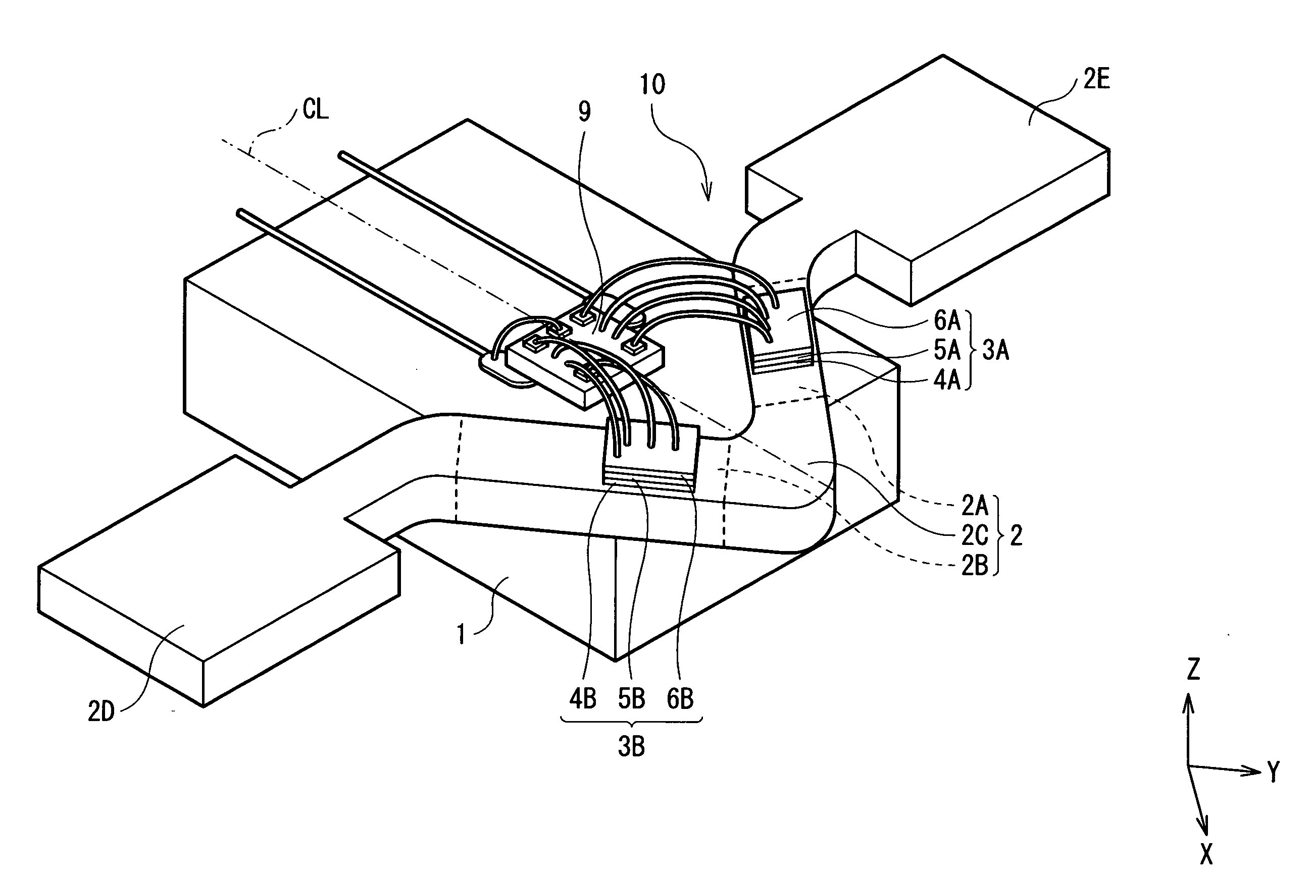
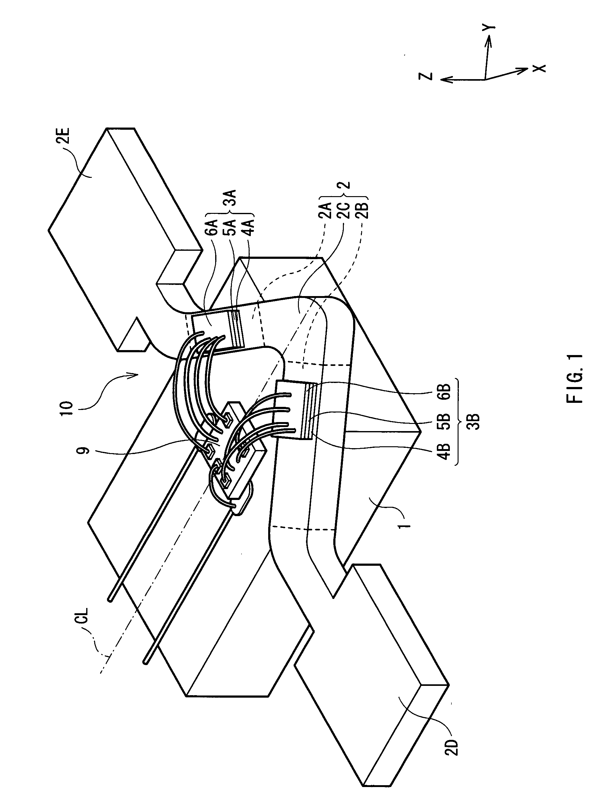
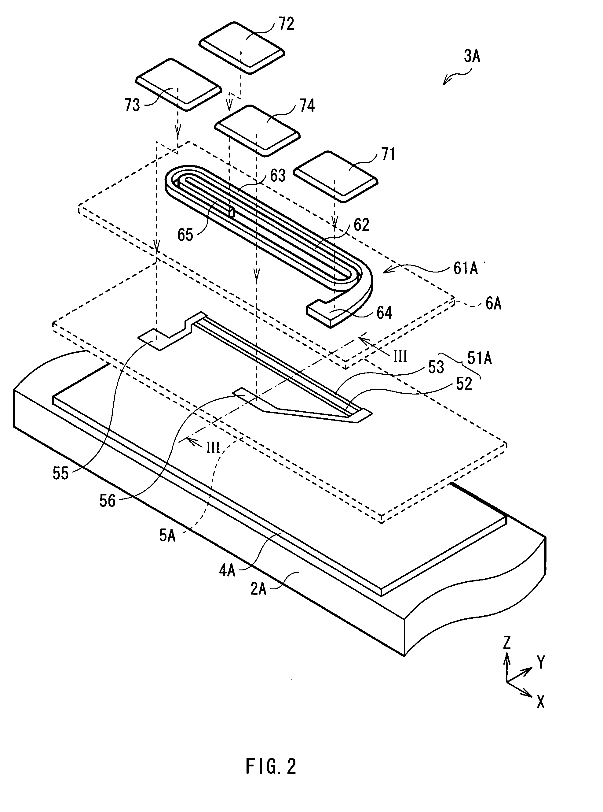
[0036]First, configuration of a current sensor as a first embodiment of the present invention will be described with reference to FIGS. 1 to 4. FIG. 1 is a schematic diagram showing a perspective configuration of a current sensor 10 according to the present embodiment, and FIG. 2 is an enlarged perspective view showing a magnetic sensor 3A (which will be described later), which is a part of the current sensor 10 of FIG. 1. FIG. 3 is a cross section of the magnetic sensor 3A shown in FIG. 2 taken along line III-III, seen from the direction indicated by the arrows. FIG. 4 illustrates a circuit configuration in the current sensor 10 shown in FIG. 1. Directions of all the arrows shown in FIG. 4, respectively representing a current to be detected Im, a compensation current Id, current magnetic fields Hm, compensation current magnetic fields Hd, bias magnetic fields Hb1 and Hb2, and a current I0, indicate a relative direction with respect to magnetoresistive elements (MR elements) 51A and...

second embodiment

[0068]Next will be explained a current sensor as a second embodiment according to the present invention. Although in the foregoing first embodiment is explained the case in which the conductor 2 of V-shaped configuration (in plan view) is used, in the present embodiment is explained a case where a straight-line shaped conductor 21 is employed.

[0069]The current sensor of the second embodiment has the same configuration as that of the above-mentioned first embodiment substantially except for the conductor 21. Namely, the current sensor of the second embodiment has the structure in which the magnetic substrates 4A and 4B, the MR element layers 5A and 5B including the MR elements 51A and 51B, and the thin film coil layers 6A and 6B are layered in this order on the straight-line-shaped conductor 21 used as a path of the current to be detected Im. Therefore, here is explained a relation of the magnetization directions J11 and J13 of the MR elements 51A and 51B (specifically the element pa...

third embodiment

[0073]Next will be explained a current sensor as a third embodiment according to the third invention. In the first embodiment as described above, the magnetic substrate 4A and the MR element layer 5A including the MR element 51A are disposed on the straight line portion 2A of the conductor 2, and the magnetic substrate 4B and the MR element layer 5B including the MR element 51B are disposed on the straight line portion 2B. In the third embodiment, on the other hand, four MR elements 51A to 51D are disposed on one conductor 2. Explanation will be made hereinbelow with reference to FIG. 8. Since its configuration is substantially similar to that of the above-mentioned first embodiment except for the point that the four MR elements 51A to 51D are disposed, descriptions will be omitted suitably according to circumstances.

[0074]FIG. 8 is a conceptual diagram showing a relation of current direction, magnetic field directions, and magnetization directions according to a current sensor of t...


PUM

PropertyMeasurementUnit
currentaaaaaaaaaa
angleaaaaaaaaaa
thicknessaaaaaaaaaa

Abstract

A current sensor capable of detecting current magnetic fields generated by a current to be detected with high precision and stability while realizing a compact configuration is provided. The current sensor includes: a conductor generating a current magnetic field in accordance with supplied current to be detected; a magnetoresistive element including a free layer having a magnetization direction that varies in accordance with the current magnetic field, a pinned layer having the magnetization direction that is pinned to a direction orthogonal to the magnetization direction of the free layer under no current magnetic field, and an intermediate layer provided between the free layer and the pinned layer; and a bias applying means for applying, to the magnetoresistive element, a bias magnetic field along a direction same with the magnetization direction of the free layer under no current magnetic field.

Description

BACKGROUND OF THE INVENTION[0001]1. Field of the Invention[0002]The present invention relates to a magnetic sensor capable of detecting a variation of a magnetic field with high sensitivity and further to a current sensor capable of detecting a variation of a current flowing through a conductor with high sensitivity.[0003]2. Description of the Related Art[0004]In measuring correctly a control current which flows through a circuit of control machinery, a method that resistances are connected in series within the circuit to measure a voltage drop of the resistances is applied in general. In this case, however, a load different from the control system is given, and there is a possibility that an adverse influence may be exerted on the control system. Consequently, a method of indirectly measuring a control current by detecting the gradient of a current magnetic field generated by the control current has been used. Specifically, a control current is supplied to a curved, U-shaped conduc...

Claims


Application Information

Patent Timeline
Patent Type & Authority Applications(United States)
IPC IPC(8): G11B5/127
CPCB82Y25/00G01R33/093G01R15/205H01L2224/48257
Inventor SHOJI, SHIGERU
Owner TDK CORPARATION
Why Eureka
Try Eureka