Electrical fuse device based on a phase-change memory element and corresponding programming method

a technology of phase-change memory and electrical fuse device, which is applied in the direction of digital storage, semiconductor devices, instruments, etc., can solve the problems of high programming voltage, large oxide thickness of modern integrated circuit, and inability to make their use totally satisfactory within modern integrated devices

Inactive Publication Date: 2007-08-16
STMICROELECTRONICS SRL
View PDF10 Cites 35 Cited by
  • Summary
  • Abstract
  • Description
  • Claims
  • Application Information

AI Technical Summary

Benefits of technology

[0014] One embodiment of the present invention is a fuse device (in particular for one-time-pro

Problems solved by technology

However, for reasons that will be briefly set forth, the solutions referred to have some problems that do not make their use totally satisfactory within modern integrated devices.
The scales of integration required by modern integrated circuits do not always enable use of such large oxide thicknesses.
Furthermore, the use of E2PROM devices in any case involves a high area occupation.
Said devices require high programming voltages, and consequently i

Method used


Image

  • Electrical fuse device based on a phase-change memory element and corresponding programming method
  • Electrical fuse device based on a phase-change memory element and corresponding programming method
  • Electrical fuse device based on a phase-change memory element and corresponding programming method

Examples


first embodiment

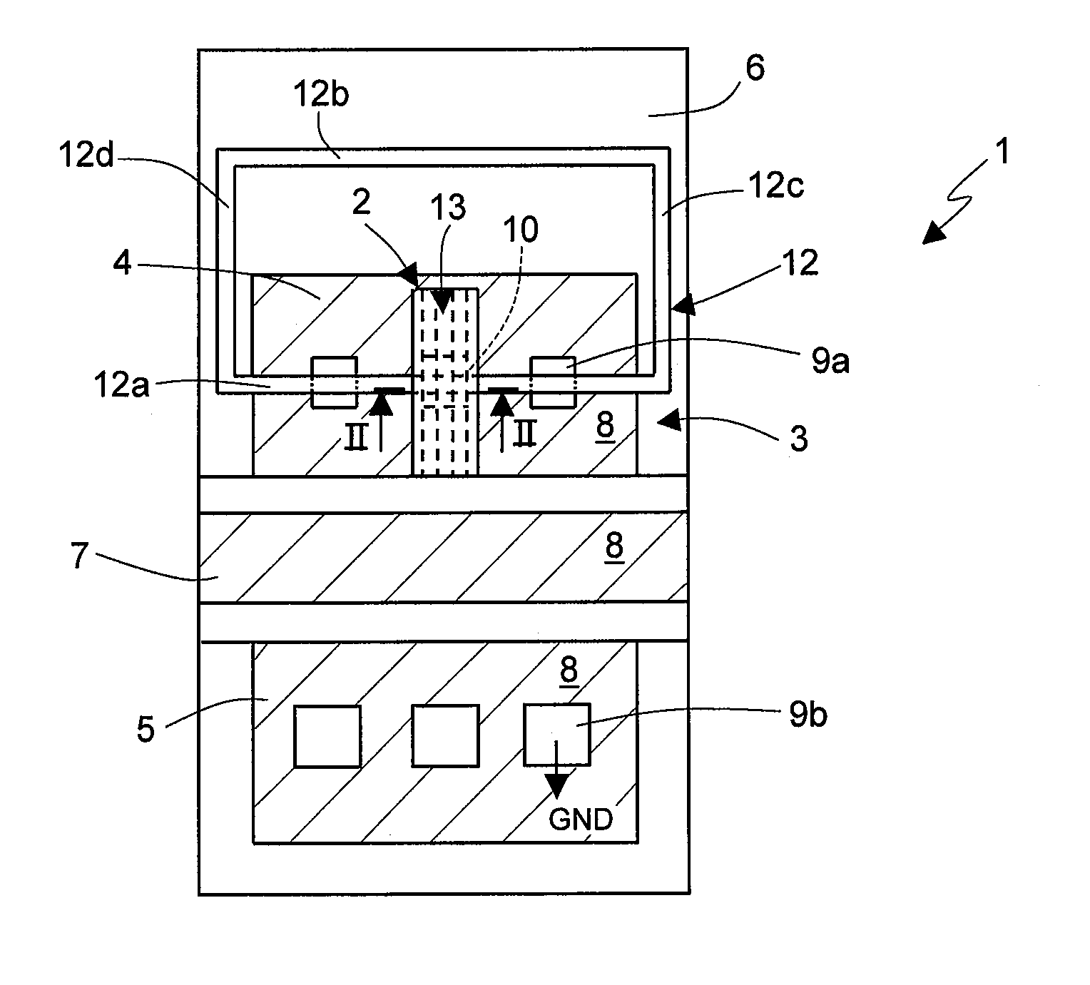
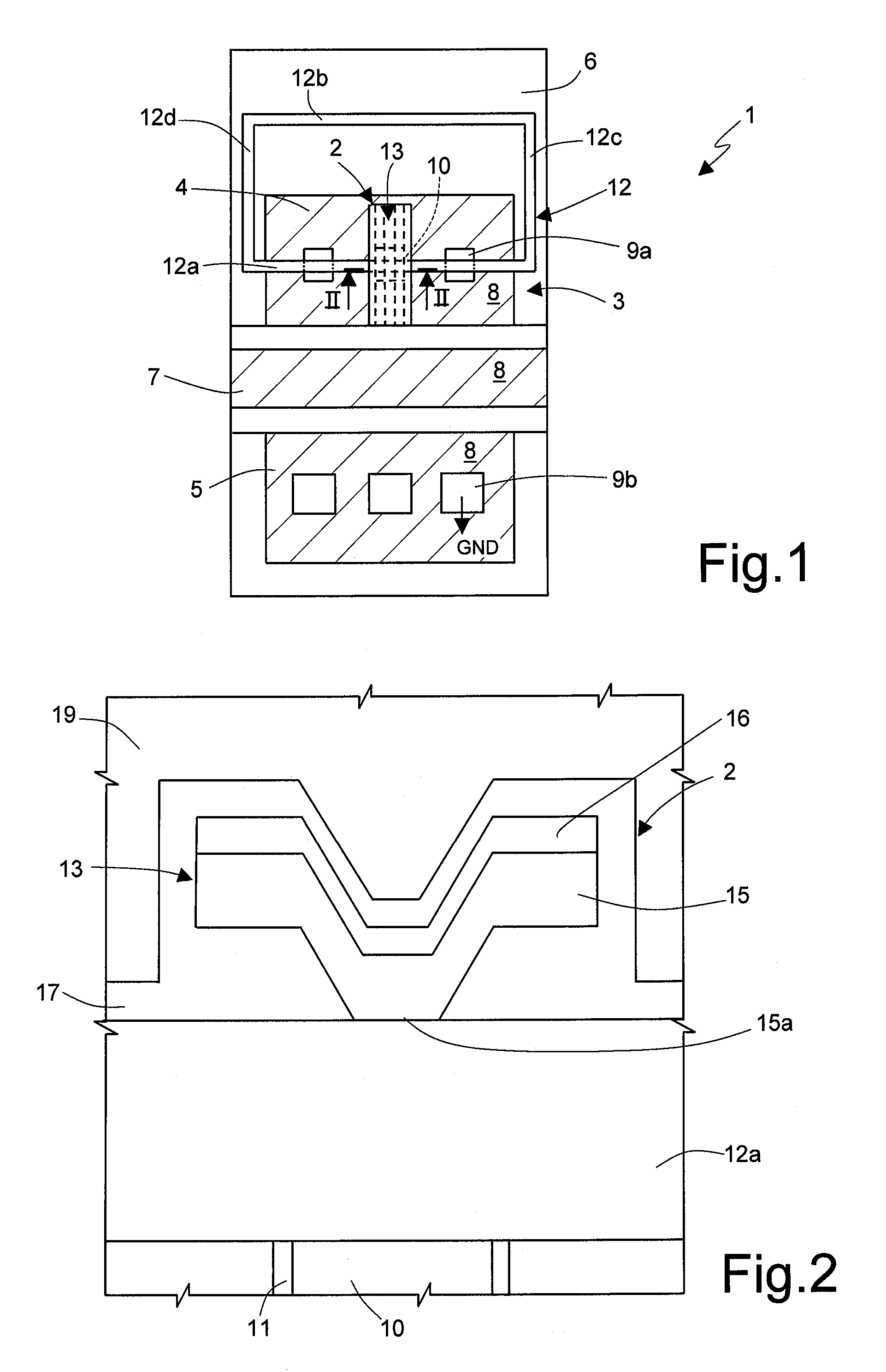
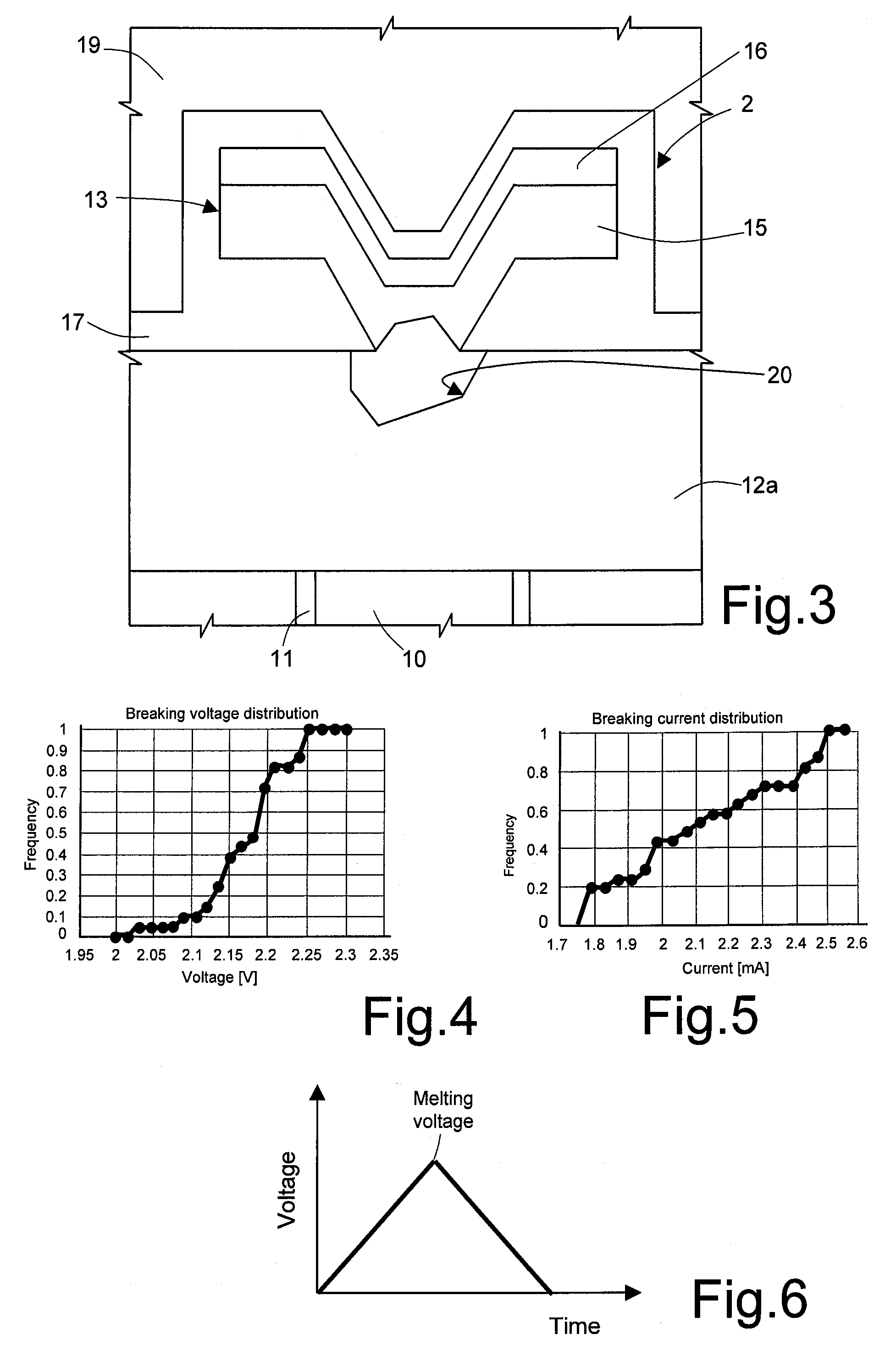
[0031] In detail, and as illustrated in FIGS. 1 and 2, a fuse device 1 according to the present invention, comprises a fuse element 2 (as will be clarified hereinafter, based on a phase-change memory element), and a selector element 3, which is electrically connected to the fuse element 2 and is configured to enable programming of the fuse element 2. In particular, by way of example, the selector element 3 illustrated in FIG. 1 is an N-channel MOSFET of a planar type. It is clear, however, that other selector elements could be used in an altogether equivalent way, for example any FET (vertical MOSFET, JFET, FinFET, etc.), or else a BJT or a BiFET. Furthermore, FIG. 1 and the following figures illustrate a phase-change memory element having a microtrench architecture. Once again, it is clear that other structures could be used in an altogether equivalent way, for example of the wall or tubular type.

[0032] In detail, the selector element 3 is provided with: a first current-conduction ...

second embodiment

[0043] A second embodiment, illustrated in FIGS. 9 and 10, envisages again the use of a selector element 3 of the planar N-channel MOSFET type, but in this case the bottom electrode 10 of the fuse element 2 is connected to the source region 5 of the selector element 3.

[0044] In detail, the selector element 3 has an active area 22, having P-type conductivity, made within the substrate 6 (having a P-doping) and isolated by means of isolation trenches 23, for example using the Shallow-Trench Isolation (STI) technique. The drain region 4 and the source region 5 are provided within the active area 22; in detail, the drain region 4 comprises a first drain strip 4a and a second drain strip 4b, which extend in a first direction x parallel to one another, and the source region 5 comprises a source strip extending in the first direction x between the drain strips 4a, 4b. In addition, electrical contacts 24 (illustrated in FIG. 9) contact the drain strips 4a, 4b. The gate region 7 is constitut...


PUM


Abstract

A fuse device has a fuse element provided with a first terminal and a second terminal and an electrically breakable region, which is arranged between the first terminal and the second terminal and is configured to undergo breaking as a result of the supply of a programming electrical quantity, thus electrically separating the first terminal from the second terminal. The electrically breakable region is of a phase-change material, in particular a calcogenic material, for example GST.

Description

BACKGROUND OF THE INVENTION [0001] 1. Field of the Invention [0002] The present invention relates to an electrical fuse device based on a phase-change memory element and to a corresponding programming method, in particular for a read-only memory (ROM) of the one-time-programmable (OTP) type, to which the following description will make reference, without this implying any loss in generality. [0003] 2. Description of the Related Art [0004] As is known, in the manufacturing process of integrated circuits, one-time-programmable ROMs find a wide range of applications for permanent storage of information, or for forming permanent connections within integrated circuits. For example, these memories can be used for programming redundant elements in order to replace identical elements that have proven faulty during an electrical testing (operation known as EWS—Electrical Wafer Sorting), prior to carrying out packaging or soldering of the integrated circuits on the board, or else for storage ...

Claims


Application Information

Patent Timeline
IPC IPC(8): G11C17/00G11C11/00
CPCG11C13/0004G11C17/16H01L23/5256H01L45/06H01L45/1233H01L45/126H01L2924/0002H01L45/144H01L27/2436H01L2924/00H10B63/30H10N70/231H10N70/8413H10N70/826H10N70/8828
Inventor PELLIZZER, FABIOTORTORELLI, INNOCENZOPIROVANO, AGOSTINOBEZ, ROBERTO
Owner STMICROELECTRONICS SRL
Why Eureka
Try Eureka