Laminate Type Thin-Film Solar Cell And Method For Manufacturing The Same

a solar cell and laminate technology, applied in the manufacture of final products, basic electric elements, solid-state devices, etc., can solve the problems of insufficient high conversion efficiency of solar cells, inability to grow semiconductor layers of good crystal structure, and inability to obtain solar cells having a sufficiently high conversion efficiency. , to achieve the effect of easy production, low waste and high efficiency

Inactive Publication Date: 2007-08-23
ROHM CO LTD
View PDF0 Cites 36 Cited by
  • Summary
  • Abstract
  • Description
  • Claims
  • Application Information

AI Technical Summary

Benefits of technology

[0015] According to the present invention, since a pair of electrodes is connected to each of a plurality of photoelectric conversion units, light of wide range of wavelength can be converted into electric power by joining the plurality of photoelectric conversion units, and by connecting the electrodes so that the plurality of photoelectric conversion units are connected in series. Moreover, since a lamination structure of the plurality of photoelectric conversion units can be formed not by continuous growth of semiconductor layers but by sticking, a lamination structure can be obtained without problems of occurrence of lattice defects caused by lattice mismatching, even if photoelectric conversion units are formed of semiconductor layers having different band gap energies and different lattice constants...

Problems solved by technology

As described above, in case of forming a tandem structure, in which light of wide range of wavelength can be absorbed, by laminating semiconductor materials having different band gap energies, since a portion of a tunnel junction is necessary, a problem occurs such that a conversion efficiency remains to be approximately 29% by a loss generated in the tunnel junction or the like.
A solar cell formed by laminating three units of InGaP, GaAs and In...

Method used


Image

  • Laminate Type Thin-Film Solar Cell And Method For Manufacturing The Same
  • Laminate Type Thin-Film Solar Cell And Method For Manufacturing The Same
  • Laminate Type Thin-Film Solar Cell And Method For Manufacturing The Same

Examples


Embodiment Construction

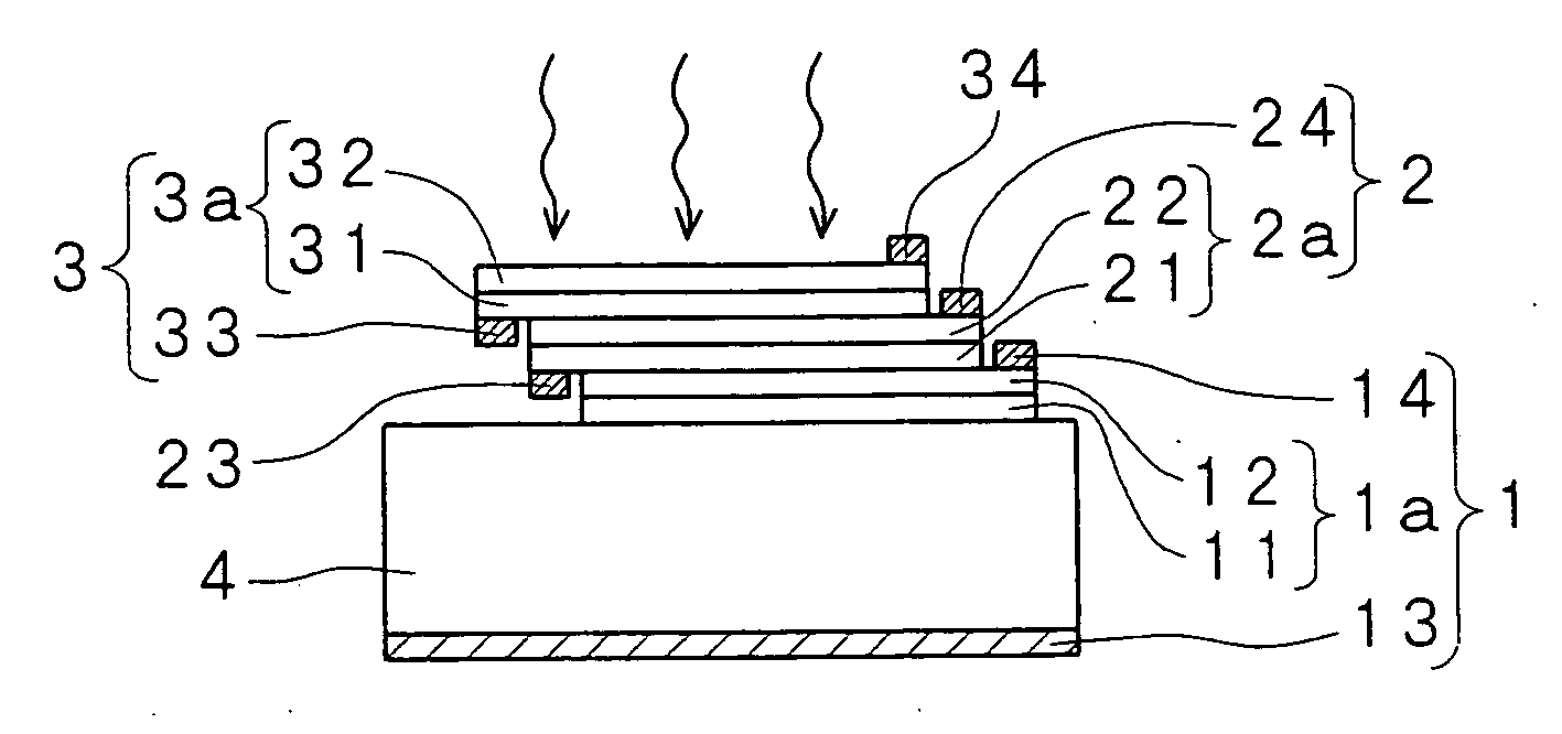
[0032] An explanation will be given below of a laminate type thin-film solar cell and a method for manufacturing the same according to the present invention in reference to FIGS. 1 to 3. The laminate type thin-film solar cell according to the present invention includes a first photoelectric conversion unit 1 formed on the substrate 4 and a second photoelectric conversion unit 2 formed on the first photoelectric conversion unit 1. The first photoelectric conversion unit 1 includes a first semiconductor lamination portion 1a (11, 12) made of a semiconductor having a first band gap energy and a first pair of electrodes 13 and 14 which are formed on at least a part of each of both surfaces of the first semiconductor lamination portion 1a and connected electrically thereto. The second photoelectric conversion unit 2 includes a second semiconductor lamination portion 2a (21, 22) made of a semiconductor having a second band gap energy and a second pair of electrodes 23 and 24 which are for...


PUM


Abstract

A laminate type thin-film solar cell which can convert sunlight efficiently into electric power and be formed in multi-laminate structure without limitation in selecting a semiconductor material, and be excellent in conversion efficiency, and a production method therefor are provided. A first photoelectric conversion unit including a first semiconductor lamination portion (1a) made of a semiconductor having a first band gap energy and a first pair of electrodes (13, 14) is provided on a substrate (4), and a second photoelectric conversion unit including a second semiconductor lamination portion (2a) made of a semiconductor having a second band gap energy and a second pair of electrodes (23, 24) is stuck thereon. A third photoelectric conversion unit including a third semiconductor lamination portion (3a) made of a semiconductor having a third band gap energy and a third pair of electrodes (33, 34) may be stuck thereon, and as many conversion units as desired can be stuck.

Description

FIELD OF THE INVENTION [0001] The present invention relates to a laminate type thin-film solar cell in which a plurality of photoelectric conversion units made of semiconductor films are laminated by sticking, and relates to a method for manufacturing the same. More particularly, the present invention relates to a laminate type thin-film solar cell capable of photoelectric conversion in high efficiency by solving a problem such as lattice defects or the like caused by a difference in lattice constants and by reducing a conversion loss caused by a tunnel junction between a plurality of photoelectric conversion units, while converting sunlight of a wide wavelength spectrum into electric power in high efficiency, and relates to a method for manufacturing the same. BACKGROUND OF THE INVENTION [0002] In a solar cell by the prior art, electrodes are formed on both sides of a p-n junction formed of, for example, silicon semiconductor, and photo-electromotive force generated at both ends of...

Claims


Application Information

Patent Timeline
IPC IPC(8): H01L31/00H01L25/04H01L31/0304H01L31/04H01L31/0687H01L31/18
CPCH01L31/03046H01L31/0687H01L31/184H01L31/1892Y02E10/544H01L2924/0002H01L31/043H01L2924/00Y02P70/50H01L31/047H01L31/0445
Inventor SAI, HIRONOBU
Owner ROHM CO LTD
Why Eureka
Try Eureka