

Light emitting device
a technology of light emitting devices and light sources, applied in the field of light emitting elements, can solve the problems of insufficient number of carriers of exciting light emitting centers, and achieve the effects of high luminous efficiency, low drive voltage, and high resistance to deterioration
- Summary
- Abstract
- Description
- Claims
- Application Information
AI Technical Summary
Benefits of technology
Problems solved by technology
Method used
Image

Examples
embodiment mode 1
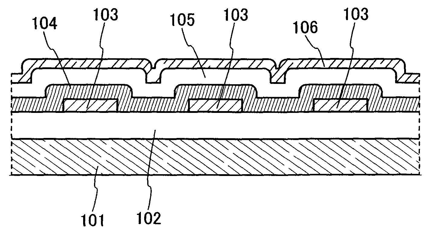
[0039]This embodiment mode describes a light emitting element of the present invention. Note that it is important in the present invention to sufficiently supply carriers to a light emitting layer in order to increase luminous efficiency of the light emitting element.
[0040]The light emitting element of the present invention has a structure shown in FIG. 1. In other words, it has a structure in which a first insulating film 102 is formed of an insulating material over a first electrode 101 made of a conductive material; a plurality of carrier supply layers 103 is partly and separately formed over the first insulating film 102; a light emitting layer 104 is formed so as to be partly in contact with the carrier supply layers 103; a second insulating film 105 is formed of an insulating material over the light emitting layer 104; and a second electrode 106 is formed of a conductive material over the second insulating film 105.
[0041]In the present invention, the light emitting layer 104 i...
embodiment mode 2
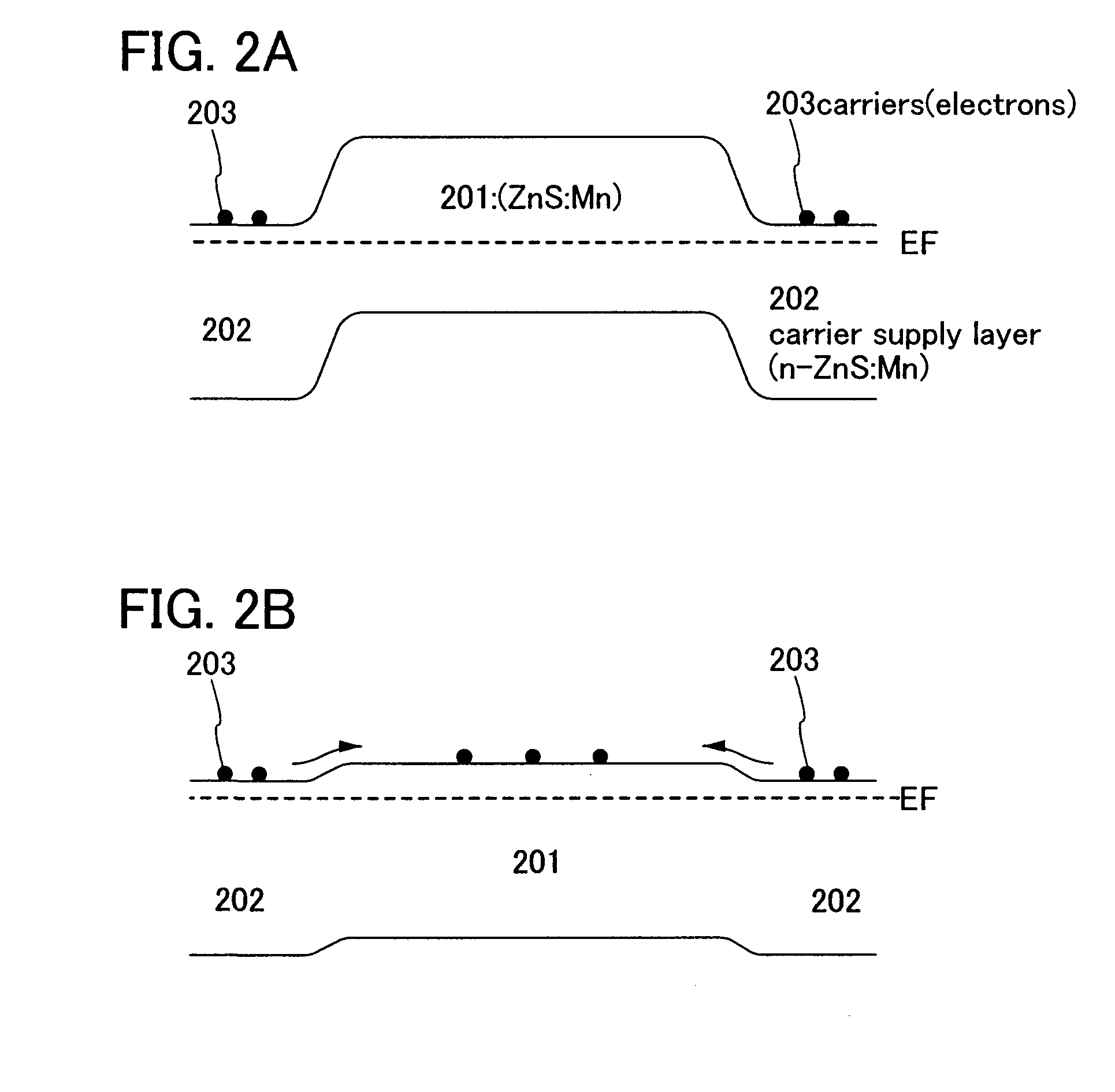
[0061]This embodiment mode describes the principle of carrier supply in a case of driving the light emitting element of the present invention.
[0062]FIG. 3 shows a structure of the light emitting element of the present invention. The light emitting element of the present invention has a structure in which a first insulating film 302 is formed of an insulating material over a first electrode 301 made of a conductive material; a plurality of carrier supply layers 303 is partly and separately formed over the first insulating film 302; a light emitting layer 304 is formed over the carrier supply layers 303; a second insulating film 305 is formed of an insulating material over the light emitting layer 304; and a second electrode 306 is formed of a conductive material over the second insulating film 305.
[0063]Note that the first electrode 301 is electrically connected to a first power source 307, and a constant voltage (reference voltage) is applied from the first power source 307 to the f...
embodiment mode 3
[0073]This embodiment mode describes an active-matrix light emitting device in which each of pixels included in a pixel portion includes a thin film transistor (TFT) and the light emitting element of the present invention.
[0074]Note that the active-matrix light emitting device can have such a circuit structure as shown in either FIG. 6A or 6B.
[0075]FIG. 6A shows a structure in which each pixel includes a single light emitting element and a single TFT functioning as a switch of the light emitting element. Therefore, the TFT shown in FIG. 6A is referred to as a switching TFT (603).
[0076]A gate electrode of the switching TFT 603 is connected to a gate line (Gj) 602. One terminal connected to a channel formation region of the switching TFT 603 is electrically connected to a source line (Si) 601, and the other terminal is electrically connected to one electrode of a light emitting element 604. Note that the other electrode of the light emitting element 604 is electrically connected to a ...
PUM
 Abstract
Description
Claims
Application Information