Display device

a display device and liquid crystal display technology, applied in non-linear optics, instruments, optics, etc., can solve the problems of power supply lines being corroded by metal corrosion, electrical short circuits, and high cost of the array substrate of the liquid crystal display panel, so as to prevent the failure of the display region

Inactive Publication Date: 2007-08-23
TOSHIBA MATSUSHITA DISPLAY TECH
View PDF0 Cites 9 Cited by
  • Summary
  • Abstract
  • Description
  • Claims
  • Application Information

AI Technical Summary

Benefits of technology

[0010] According to the present invention, the cut portion for electrically cutting the first wire portion in the vicinity of the edge portion of the first substrate of the first wire portion is provided to the first wire portion out of the first wire portion and the second wire portion which are provided so as to be adjacent to each other over the region from the display region between the first substrate and the second substrate to the edge portion of the first substrate, whereby the cut portion serves as an end portion at which the potential of the first wire portion arises. Accordingly, the distance between the end portions at the display region side of the first wire portion and the second wire portion at which differential potentials occur can be increased. Therefore, the electrical short-circuit between the first wire portion and the second wire portion can be prevented, and the metal corrosion of the portion of the first wire portion at the display region side from the cut portion can be prevented, so that a display failure in the display region can be prevented.

Problems solved by technology

Particularly, the array substrate of the liquid crystal display panel is very expensive, and rigorously checked after passing through a process of manufacturing the array substrate.
Therefore, when current is supplied to the liquid crystal display panel under a high-humidity atmosphere, an electrical short-circuit may occur between power supply lines to which different voltages are applied, or the power supply lines may suffer metal corrosion, that is, electrical corrosion may occur.
Accordingly, some display failure may occur in an image which is displayed in the image display region.

Method used


Image

  • Display device
  • Display device
  • Display device

Examples


first embodiment

[0021] The construction of a display device according to the present invention will be described with reference to FIG. 1 to FIG. 5.

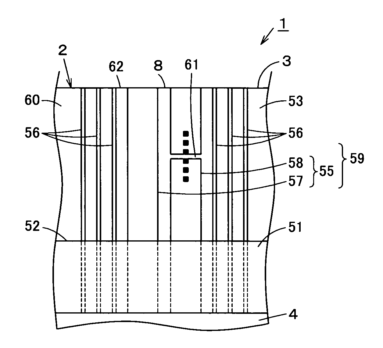
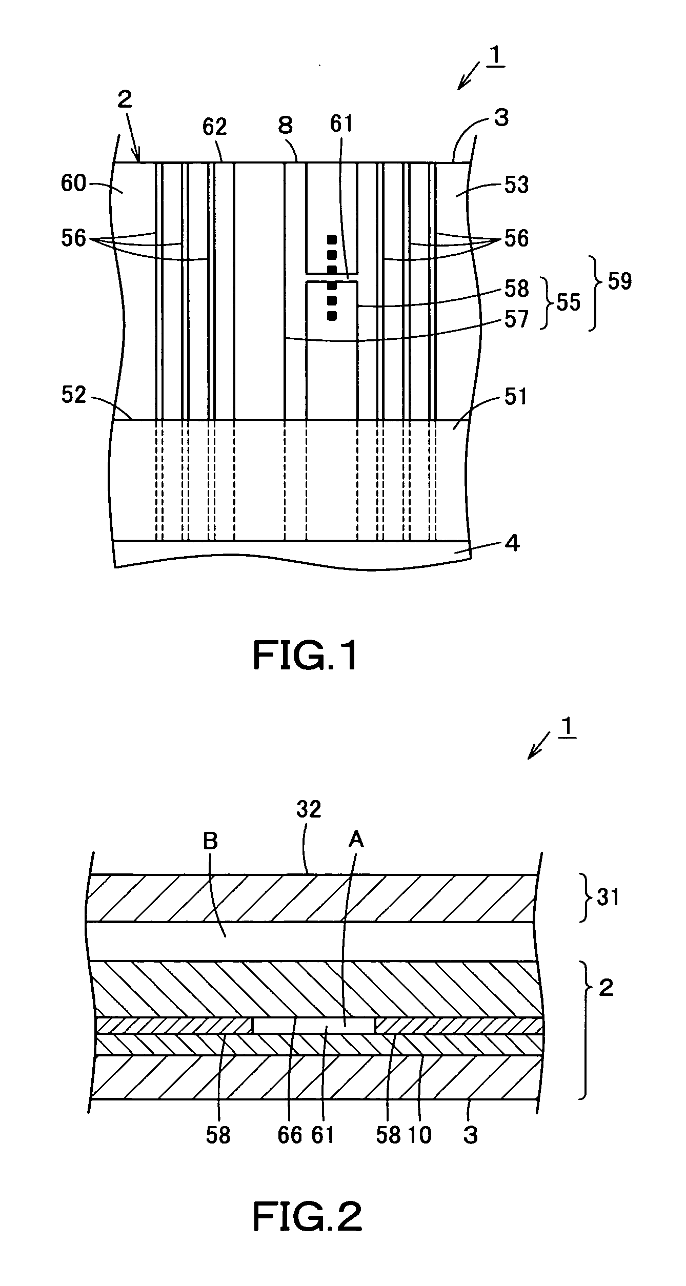
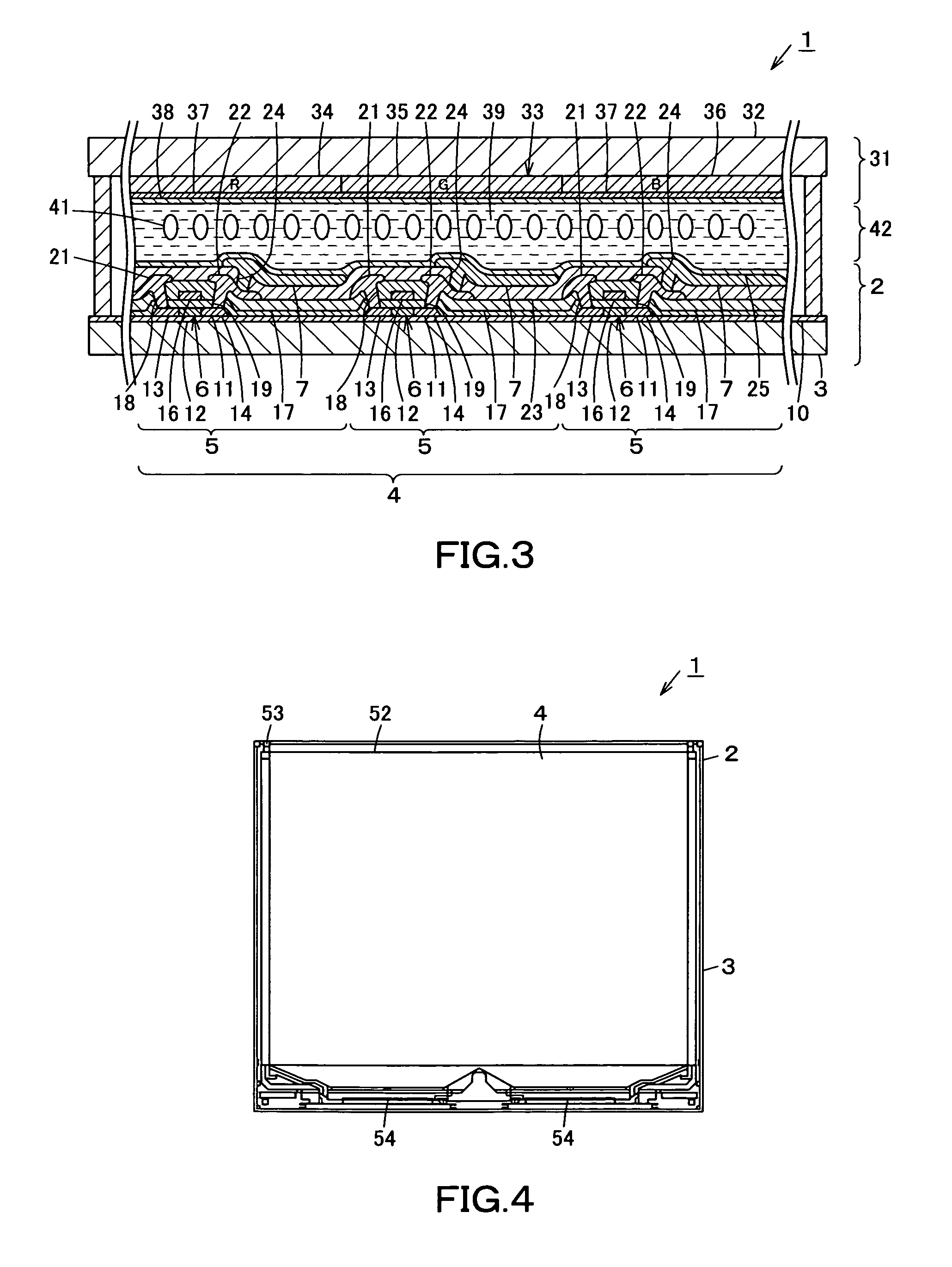
[0022] In FIG. 1 to FIG. 5, reference numeral 1 represents a liquid crystal display panel as a display device. The liquid crystal display panel 1 is an active matrix type and reflection type liquid crystal display device. The liquid crystal display panel 1 has a substantially rectangular flat plate type array substrate 2 as a thin film transistor (TFT) substrate. The array substrate 2 has a glass substrate 3 as a substantially transparent rectangular flat plate type first substrate having both insulation property and translucent property. An image display region 4 which is rectangular in plan view and serves as a display region portion covering the center portion of the surface of the glass substrate 3 is provided at the center portion on the surface corresponding to one principal surface of the glass substrate 3. The image display region 4 is a region ...

third embodiment

[0064] Furthermore, as in the case of a third embodiment shown in FIG. 8 and FIG. 9, polymer resin is patterned on the insulating layer 66 laminated on the wire region 53 of the mother substrate 63 to laminate a polymer resin layer 72 as a protection layer, whereby the dummy metal wires 56, the high voltage power supply wire 57 and the low voltage power supply wire 58 which are wired in the wire region 53 are covered by the polymer resin layer 72. That is, the polymer resin layer 72 is provided over the region extending from the outer edge of the seal region 51 of the glass substrate 3 of the array substrate 2 to the end face of the glass substrate 3 which corresponds to the outer edge of the wire region 53.

[0065] The polymer resin layer 72 is formed of organic film which is not damaged and melted by irradiation of the laser beam to be irradiated when the wire cut portion 61 is formed in the low voltage power supply wire 58, and through which no laser beam is transmitted. Furthermor...

fourth embodiment

[0069] Furthermore, in each of the above-described embodiments, the liquid crystal display panel 1 uses the liquid crystal layer 42 as the optical modulation layer, however, an organic EL display panel 75 may be used as a display device using an organic EL (electroluminescence) layer 74 as a light emitting layer as in the case of a fourth embodiment shown in FIG. 10. The organic EL display panel 75 is equipped with an active matrix substrate 76 as a TFT substrate, and a sealing substrate 77 as cap glass. The active matrix substrate 76 and the sealing substrate 77 are disposed so as to face each other via a predetermined gap, and the outer peripheral edges thereof are adhesively attached to each other by seal agent 52. Furthermore, the space portion 78 between the active matrix substrate 76 and the sealing substrate 77 which is hermetically sealed by the seal agent 52 is filled with inert gas such as argon (Ar) gas, nitrogen (N2) gas or the like.

[0070] The active matrix substrate 76 ...


PUM

PropertyMeasurementUnit
voltageaaaaaaaaaa
voltageaaaaaaaaaa
voltageaaaaaaaaaa

Abstract

An intermediate portion of a low voltage power supply wire is extinguished by irradiation of a laser beam to form a wire cut portion. A different potential portion serves as the wire cut portion of the low voltage power supply wire. The distance between the end portions of a high voltage power supply wire and the low voltage power supply wire between which the potential is different is increased. An electrical short-circuit between the high voltage power supply wire and the low voltage power supply wire hardly occurs. Even when impurities invade into the gap between an insulating layer on the high voltage power supply wire and the low voltage power supply wire and a glass substrate, electrode corrosion of the high voltage power supply wire and the low voltage power supply wire can be prevented. A display failure can be prevented.

Description

INCORPORATION BY REFERENCE [0001] The present invention claims priority under 35 U.S.C. §119 to Japanese Patent Application No. 2006-007357 filed on Jan. 16, 2006. The content of the application is incorporated herein by reference in its entirety. FIELD OF THE INVENTION [0002] The present invention relates to a display device having a display region between a first substrate and a second substrate. BACKGROUND OF THE INVENTION [0003] A flat panel display as this type of display device is very excellent in space saving, convenience and portability, and it is broadly used in a multimedia terminal as a liquid crystal display, organic EL (electroluminescence) display or the like. [0004] An active type display driving technique has been mainly applied to the liquid crystal display and the organic EL display in order to implement excellent reproduction of pictures and information. The liquid crystal display is constructed by a liquid crystal display panel in which a counter substrate is di...

Claims


Application Information

Patent Timeline
Patent Type & Authority Applications(United States)
IPC IPC(8): G02F1/1333
CPCG02F2001/136254G02F1/1345G02F1/136254
Inventor MIYASHITA, KIYOSHIMATSUNAGA, IKUOISHIMARU, MASASHINAKAWAGA, YOSHIHITOSETO, MASAKIHANARI, JUN
Owner TOSHIBA MATSUSHITA DISPLAY TECH
Why Eureka
Try Eureka