Apparatus and method for plasma etching
- Summary
- Abstract
- Description
- Claims
- Application Information
AI Technical Summary
Benefits of technology
Problems solved by technology
Method used
Image

Examples
embodiment 1
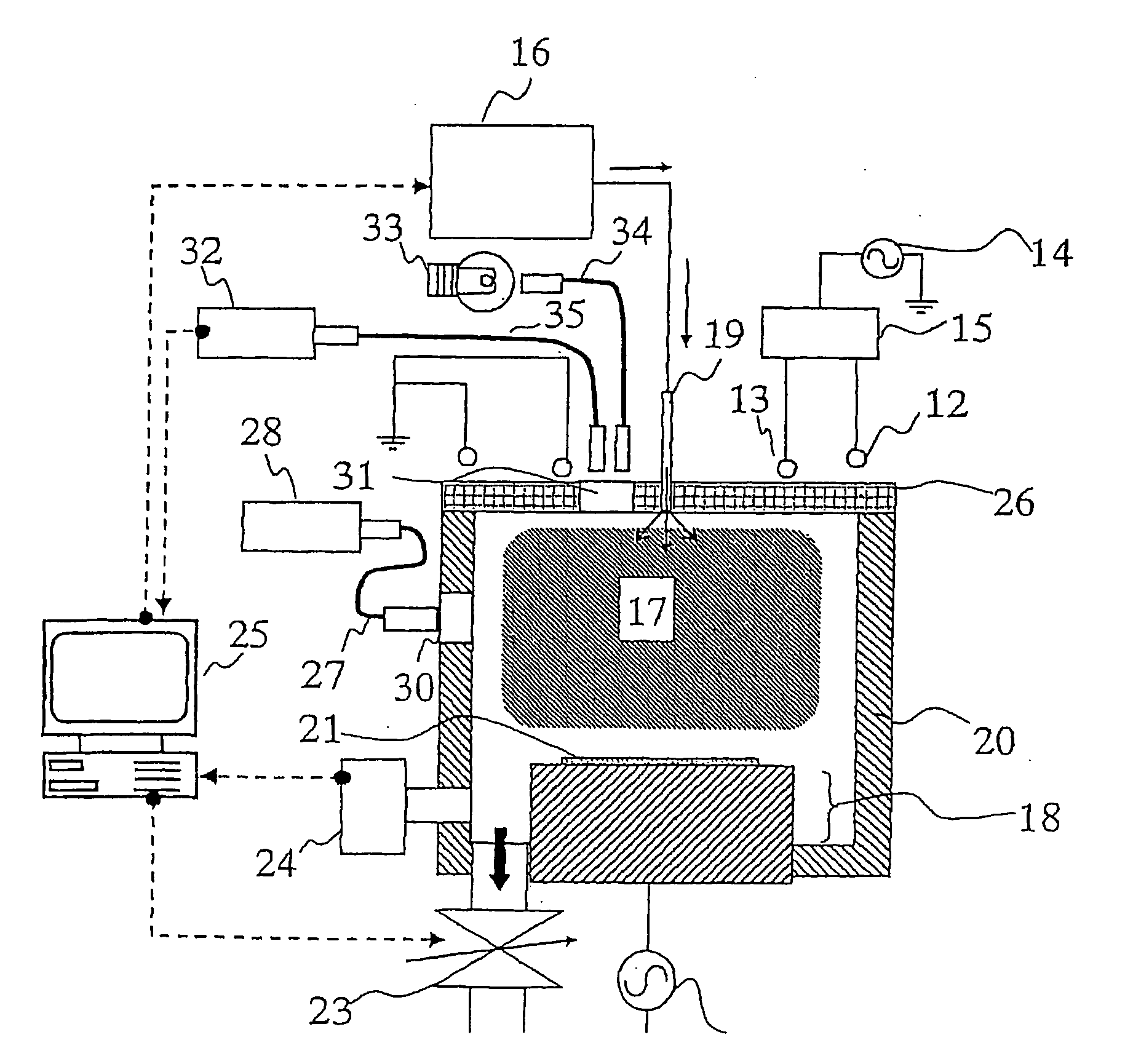
[0062]The structure of an etching apparatus according to embodiment 1 of the present invention is illustrated in FIG. 1. In this apparatus, etching gas is supplied from a gas supply unit 16 via a gas nozzle 19 into a vacuum processing chamber 20, and an RF power of 13.56 MHz is applied from an RF (high frequency) power supply 14 to antenna coils 13 and 12 disposed outside a dielectric window 26 formed of alumina, to thereby generate inductively coupled plasma 17 from the etching gas.
[0063]A power distributor 15 is disposed between the antenna coils 12 and 13 and the RF power supply 14, so as to control the distribution of the generated plasma by adjusting the ratio of power supply to the antenna coils 12 and 13. The etching process is performed by irradiating plasma to a wafer 21 mounted on a wafer stage 18. An RF power supply 29 is connected to the wafer stage 18, and the wafer 21 is etched effectively by applying an RF power of 13.56 MHz thereto.
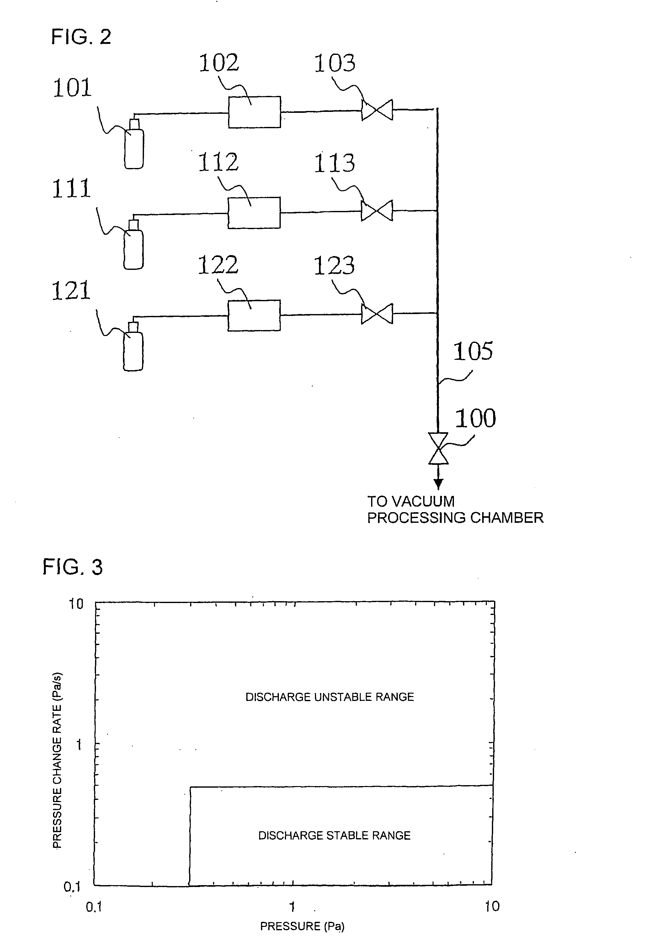
[0064]Furthermore, the pressure of ...
embodiment 2
[0077]When utilizing the method of embodiment 1 to continuously process two wafers by performing continuous discharge while switching the types of gases, the flow rates of gases and the pressures of gases according to a three-step etching shown in FIG. 6, there had been discovered a phenomenon in which the finished sizes of the first wafer and the second wafer differ greatly.
[0078]FIG. 7 shows the time variation of the total gas flow rate during processing of the first wafer, and FIG. 8 shows the time variation of the total gas flow rate for the second wafer. In the wafer processing of the first wafer shown in FIG. 7, during the first three seconds of the start of flow of the second gas 111 and the first three seconds of the start of flow of the third gas 121, the gas flow rate varied greatly and became unstable. In contrast, during processing of the second wafer shown in FIG. 8, such unstable gas flow rate is not seen during the start of flow of gas 111 or the start of flow of gas ...
embodiment 3
[0084]According to the system of embodiment 2, it is possible to perform continuous discharge having an improved reproducibility without any instability during switching of conditions including the processing of first and second wafers, but even according to the system of embodiment 2, there were cases in which the finished product was defective.
[0085]The product defectiveness of the wafer was examined in detail, and it has been found that the product defect rate caused by particles when the system of embodiment 2 was used to perform continuous discharge sometimes even reached 70%, which is equivalent to the case in which the discharge was performed intermittently.
[0086]With the aim to solve the above-mentioned problem, FIG. 12 shows the result of examination of the time variation of reflecting power with respect to the example of FIG. 10. In FIG. 12, it can be seen that the reflective power is instantaneously increased immediately subsequent to transiting from step 1 to step 2 and ...
PUM
| Property | Measurement | Unit |
|---|---|---|
| Time | aaaaa | aaaaa |
| Thickness | aaaaa | aaaaa |
| Pressure | aaaaa | aaaaa |
Abstract
Description
Claims
Application Information
 - R&D
- Intellectual Property
- Life Sciences
- Materials
- Tech Scout
- Unparalleled Data Quality
- Higher Quality Content
- 60% Fewer Hallucinations
Browse by: Latest US Patents, China's latest patents, Technical Efficacy Thesaurus, Application Domain, Technology Topic, Popular Technical Reports.
© 2025 PatSnap. All rights reserved.Legal|Privacy policy|Modern Slavery Act Transparency Statement|Sitemap|About US| Contact US: help@patsnap.com