Gallium nitride material transistors and methods for wideband applications

a technology of gallium nitride and transistor, applied in the direction of semiconductor devices, electrical equipment, chemical instruments and processes, etc., can solve the problems of difficult to grow high-quality gallium nitride materials on certain substrates, difficult to form gallium nitride material devices meeting the property requirements of certain applications, and applications for rf power transistors may have particularly demanding property requirements

Inactive Publication Date: 2007-08-30
INTERNATIONAL RECTIFIER COEP
View PDF81 Cites 17 Cited by
  • Summary
  • Abstract
  • Description
  • Claims
  • Application Information

AI Technical Summary

Benefits of technology

[0007] In one aspect, a device adapted to receive an input signal and to transmit an output signal is provided. The device comprises at least one transistor structure to receive the input signal. The at least one transistor includes at least one active region formed in a gallium nitride material region. The at least one transistor structure is adapted to amplify the input signal to form the output signal. The output signal, when transmitted, has an RCE of less than or equal to −10 dB.
[0008] In another aspect, a device for generating a radio frequency (RF) output signal from an RF input signal is provided. The device comprises at least one transistor having at least one active region formed in a gallium nitride material layer. The at least one transistor arranged to receive the RF input signal and, when present, amplify the RF input signal to provide the RF output signal. The device includes at least one matching circuit adapted to transform at least one impedance of the device such that, when the device is loaded with a load, the RF output signal is capable of being transmitted with an RCE of less than or equal to −10 dB.
[0009] In another aspect, a method of generating an output signal for wireless transmission is provided. The method comprises receiving an input signal comprising information to be transmitted. The method further comprises amplifying the input signal via at least one transistor structure having at least one active region formed in a gallium nitride material region to provide the output signal. The method further comprises transmitting the output signal such that the output signal has an RCE of less than or equal to −10 dB.

Problems solved by technology

Despite the attractive properties noted above, a number of challenges exist in connection with developing gallium nitride material-based devices.
For example, it may be difficult to grow high quality gallium nitride materials on certain substrates, particularly silicon, due to property differences (e.g., lattice constant and thermal expansion coefficient) between the gallium nitride material and the substrate material.
Also, it is has been challenging to form gallium nitride material devices meeting the property requirements for certain applications.
Applications for RF power transistors may have particularly demanding property requirements.

Method used


Image

  • Gallium nitride material transistors and methods for wideband applications
  • Gallium nitride material transistors and methods for wideband applications
  • Gallium nitride material transistors and methods for wideband applications

Examples


example 1

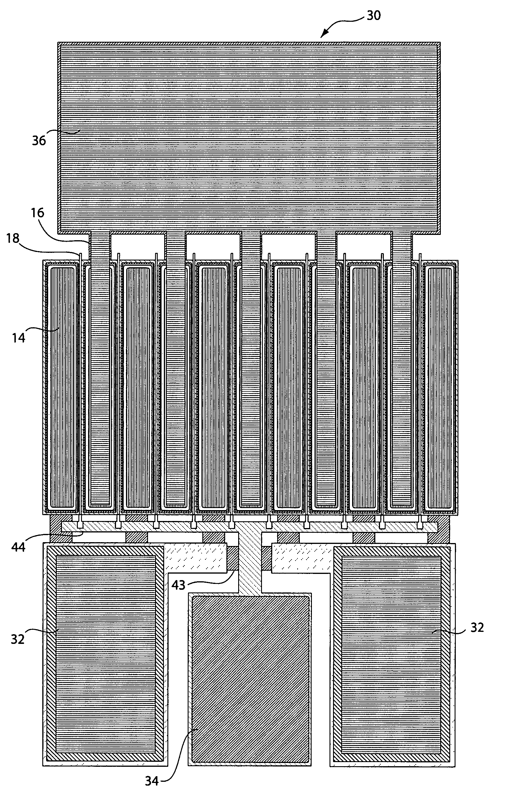
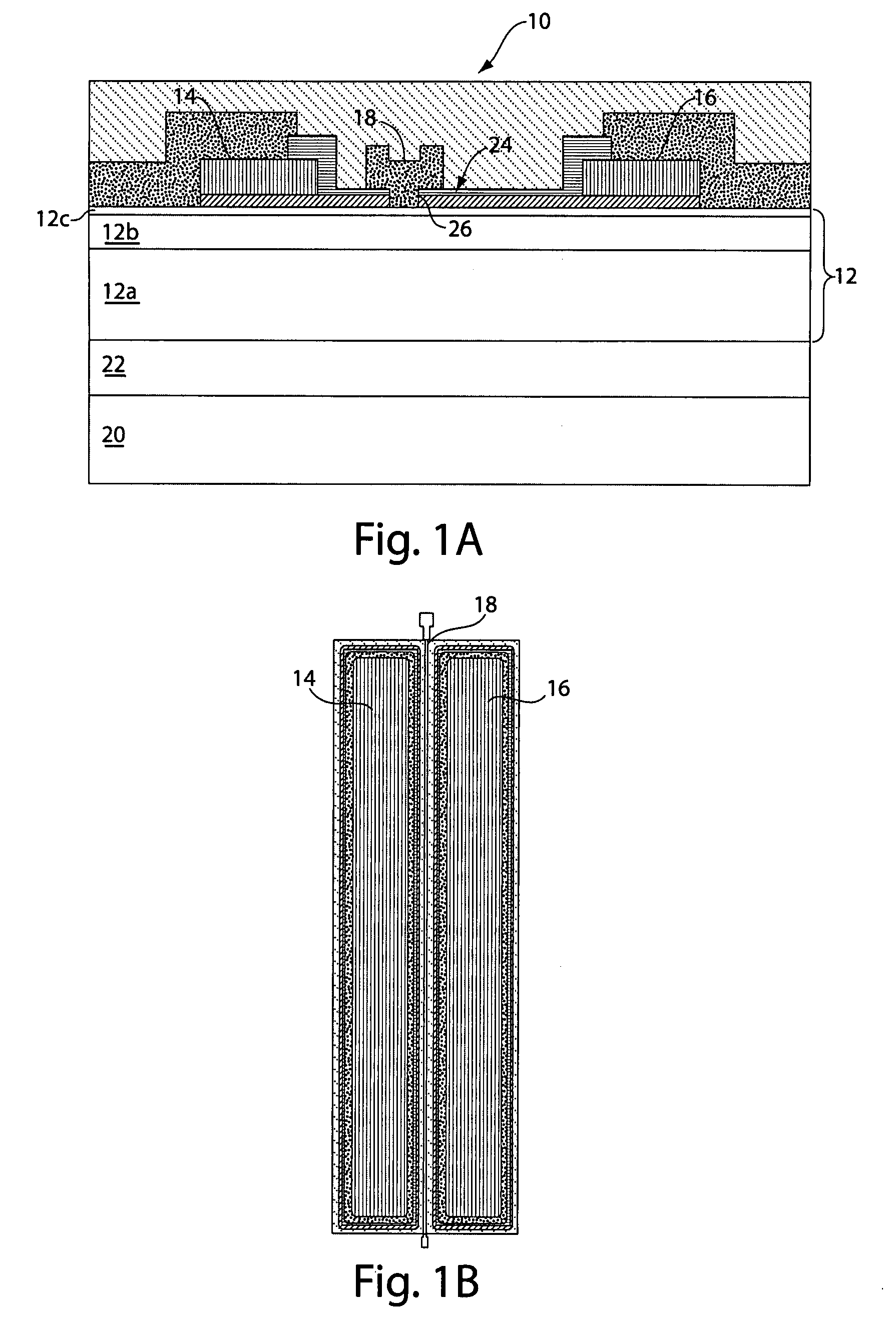
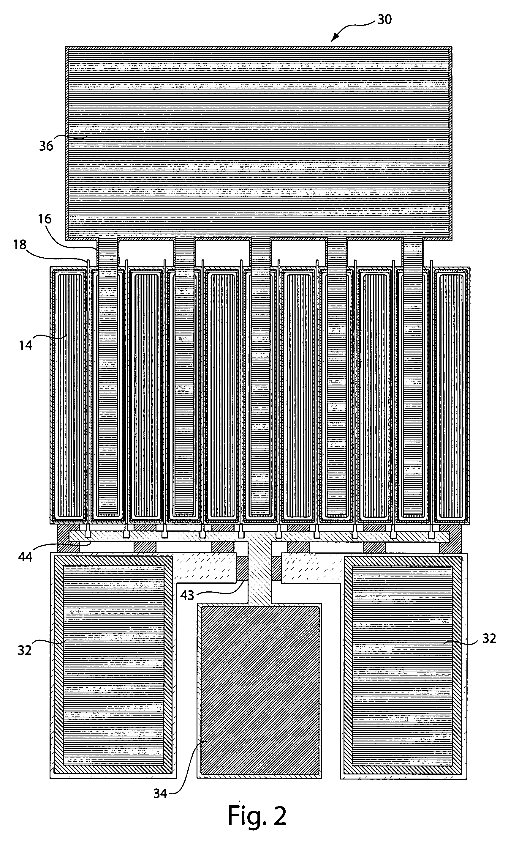
[0106] A high electron mobility transistor (HEMT) having a design similar to the structures illustrated in FIGS. 1-3 was manufactured and tested. The transistor included a gallium nitride material region formed on a silicon substrate.

[0107] The transistor was designed for operating at 3.3-3.9 GHz (WiMAX applications). The following test conditions were used (unless otherwise noted): case temperature of 25±3 degrees Celsius; single carrier OFDM waveform 64-QAM ¾; 8 burst; 20 msec frame; 15 msec frame data; 3.5 MHz channel bandwidth; Peak / Avg=10.3 dB @ 0.01% probability on CCDF; frequency=3400-3600 MHz; Pout=38 dBm; Vdd=28V; Idq=750 mA.

[0108]FIGS. 7A-7L show the results of the testing. FIG. 7A shows OFDM performance measured in a demonstration board (3400 & 3600 MHz). FIG. 7B shows ETSI mask compliance measured in a demonstration board. FIG. 7C shows OFDM performance at Pout=38 dBm in a Load Pull System (3300-3800 MHz). FIG. 7D shows OFDM performance at 3500 MHz vs. IDQ. FIG. 7E sho...


PUM

PropertyMeasurementUnit
impedanceaaaaaaaaaa
impedanceaaaaaaaaaa
frequenciesaaaaaaaaaa

Abstract

Gallium nitride material transistors and methods associated with the same are provided. The transistors may be used in power applications by amplifying an input signal to produce an output signal having increased power. The transistors may be designed to transmit the majority of the output signal within a specific transmission channel (defined in terms of frequency), while minimizing transmission in adjacent channels. This ability gives the transistors excellent linearity which results in high signal quality and limits errors in transmitted data. Such properties enable the transistors to be used in RF power applications including wideband power applications (e.g., WiMAX, WiBRO, and others) based on OFDM modulation.

Description

RELATED APPLICATIONS [0001] This application claims priority to U.S. Patent Application Ser. No. 60 / 723,824, filed on Oct. 4, 2005 which is incorporated herein by reference.FIELD OF INVENTION [0002] The invention relates generally to gallium nitride material devices and, more particularly, to gallium nitride material transistors and methods associated with the same. BACKGROUND OF INVENTION [0003] Gallium nitride materials include gallium nitride (GaN) and its alloys such as aluminum gallium nitride (AlGaN), indium gallium nitride (InGaN), and aluminum indium gallium nitride (AlInGaN). These materials are semiconductor compounds that have a relatively wide, direct bandgap which permits highly energetic electronic transitions to occur. Gallium nitride materials have a number of attractive properties including high electron mobility, the ability to efficiently emit blue light, and the ability to transmit signals at high frequency, amongst others. Accordingly, gallium nitride materials ...

Claims


Application Information

Patent Timeline
Patent Type & Authority Applications(United States)
IPC IPC(8): B32B9/00
CPCH01L29/2003H01L29/7787H01L29/42316H01L29/41758H01L29/778H01L21/18H01L27/06
Inventor CHAUDHARI, APURVA D.MARQUART, JEFFREYNAGY, WALTER H.LINTHICUM, KEVIN J.
Owner INTERNATIONAL RECTIFIER COEP
Why Eureka
Try Eureka