

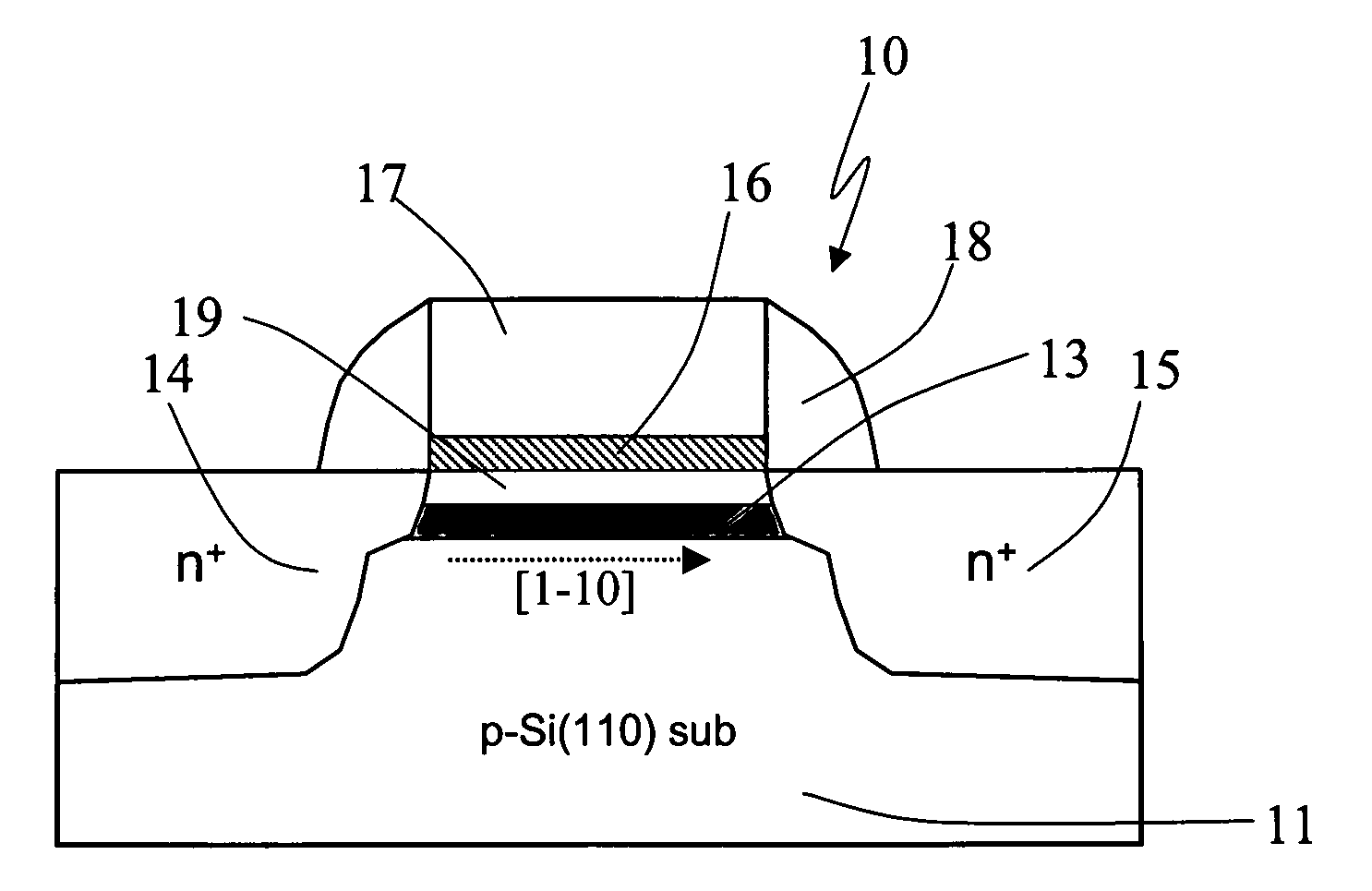
Architecture of a n-type metal-oxide-semiconductor transistor with a compressive strained silicon-germanium channel fabricated on a silicon (110) substrate
a metal-oxide-semiconductor transistor and nmos technology, applied in the direction of transistors, electrical devices, semiconductor devices, etc., can solve the problems of high fabrication cost, low efficiency, and inability to improve the cmos transistor by using silicon (110) substrate optimally, so as to improve the electrical performance of the nmosfet element, promote the mobility of electrons, and improve the electrical performance. effect of the nmos
- Summary
- Abstract
- Description
- Claims
- Application Information
AI Technical Summary
Benefits of technology
Problems solved by technology
Method used
Image

Examples
Embodiment Construction
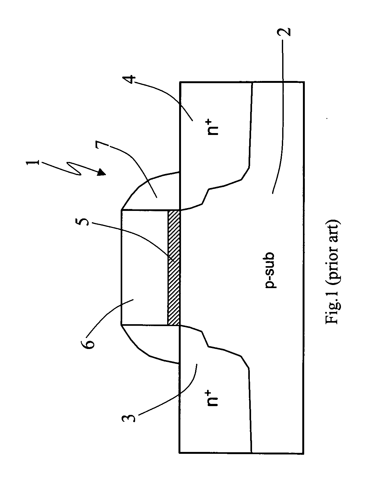
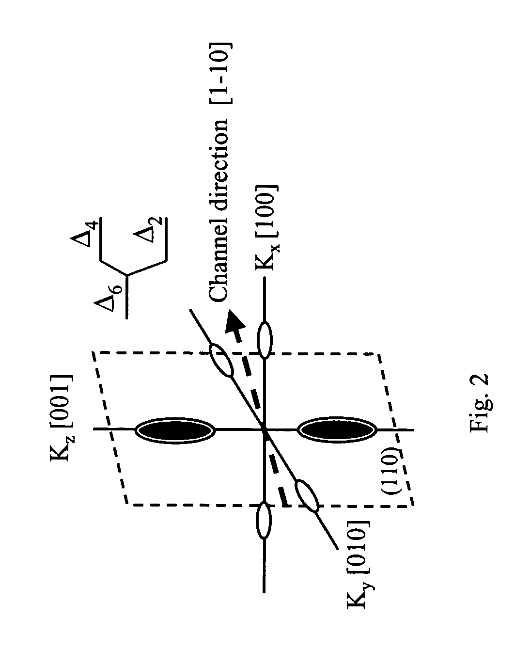
[0017] The MOS elements used in various electronic devices can be briefly divided into high-speed MOS elements and low-power-consumption MOS elements. At present, the strained-Si technology was employed to fabricate the MOSFETs, because an appropriate strain can enhance the carrier mobility in the Si channel. Further, different strains, such as a tensile strain and a compressive strain, have different influences on the mobilities of electrons and holes in different crystallographic directions on different crystallographic planes.
[0018] Several embodiments of the present invention will be described in detail below in order to prove the efficacy of the present invention, wherein a compressive strained Si—Ge channel layer is grown on the crystallographic plane (110) of a p-silicon substrate to promote the electron mobility of NMOS transistors.
[0019] The present invention proposes an architecture of a NMOS transistor with a strained Si—Ge channel in p-silicon (110) substrate. An archi...
PUM
 Abstract
Description
Claims
Application Information