Semiconductor device, and power supply device and image pickup device using the same

Inactive Publication Date: 2007-09-06
ROHM CO LTD
View PDF3 Cites 0 Cited by
  • Summary
  • Abstract
  • Description
  • Claims
  • Application Information

AI Technical Summary

Benefits of technology

[0014] Furthermore, preferred embodiments of the present invention effectively minimize the incoming current that is generated at the start of the power supply device while also minimizing an increase in the package size or chip area.
[0031] The preferred embodiments of the present invention make it possible to switch the negative-side circuit on and off by using a switch input as a single power supply voltage without depending on a positive power supply voltage as is necessary in the prior art.
[0032] Because the positive power supply voltage is not required for the operation of the switch, there is no restriction on the order of the application of the power supplies. Accordingly, there is no program or circuit necessary to set the input order, so that the design of electrical devices using the preferred embodiments of the present invention is facilitated.
[0033] In addition, with the power supply device of the preferred embodiments of the present invention, it is possible to effectively minimize the incoming current that is generated at the start of the power supply device while also minimizing an increase in the package size or chip area.

Problems solved by technology

Immediately following this start, however, an excessive incoming current flows at one time to an uncharged smoothing capacitor that is connected to the output terminal, so that there is a concern of causing abnormal heat generation or damage to the circuit elements (see FIG. 10A).
However, in the arrangement of FIG. 11A, although it is possible to gain a sufficient soft-start time by externally connecting a capacitor Ca having a large capacitance, a dedicated pin Tc for externally connecting one end of the capacitor Ca is required, so that there is a problem in that a reduction in the package size is inhibited.
Moreover, in the arrangement of FIG. 11B, although an increase in the number of pins can be avoided, it is necessary to increase the capacitance of the capacitor Cb installed inside the integrated circuit in order to gain a sufficient soft-start time, which leads to the problem of an increase in the chip area.
In the arrangement of FIG. 11B, however, while the soft-start time can also be extended by making the current value of the constant current source Ib very small, if the current value of the constant current source Ib is reduced to an extremely small value, the effect of high-temperature leaks or the like is increased, so that it is difficult to achieve the soft-start time.
However, the prior art in Patent Reference 2 is a technique used to make the soft-start time constant without depending on the input voltage Vin at all, and is not devised with a reduction in the package size or chip area in mind.

Method used


Image

  • Semiconductor device, and power supply device and image pickup device using the same
  • Semiconductor device, and power supply device and image pickup device using the same
  • Semiconductor device, and power supply device and image pickup device using the same

Examples


first preferred embodiment

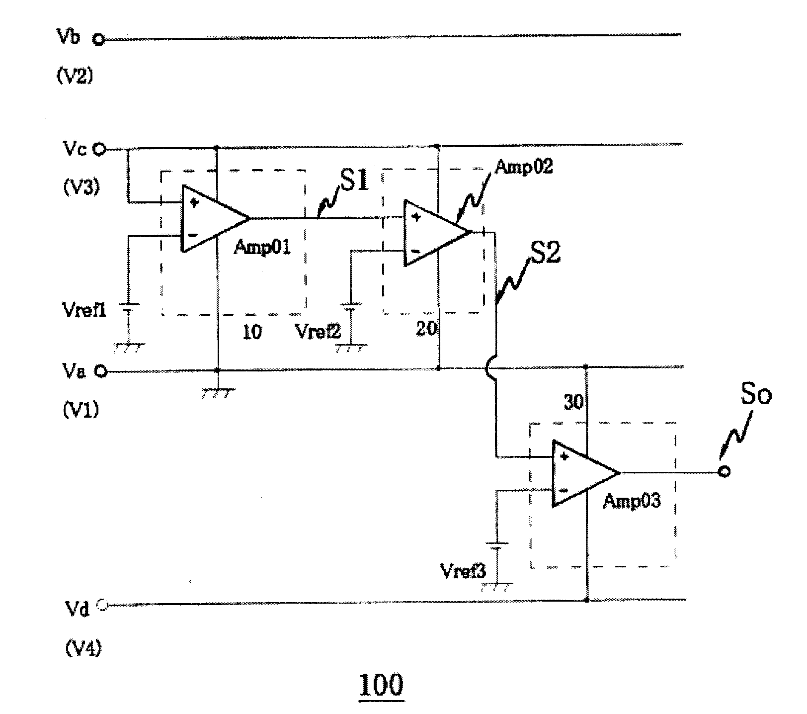
[0047]FIG. 1 is a diagram showing a first preferred embodiment of a semiconductor device 100 of the present invention. The semiconductor device 100 includes a detection circuit 10, an auxiliary circuit 20, and a signal output circuit 30. A first voltage V1 (e.g., 0 V) is applied to a first terminal Va. A second voltage V2 (e.g., 5 V) is applied to a second terminal Vb. A third voltage V3 which is equal to or higher than the first voltage V1 and which is equal to or lower than the second voltage V2 is applied to a third terminal Vc. A fourth voltage V4 (e.g., −5 V) is applied to a fourth terminal Vd. The relative magnitudes of the respective voltages is such that V2≧V3≧V1>V4.

[0048] The detection circuit 10 is defined by, for instance, a comparator or an error amplifier Amp01; the third terminal Vc is connected to the non-inverting input terminal thereof, while a constant voltage source for producing a first reference voltage Vref1 that is a specified voltage between the first voltag...

second preferred embodiment

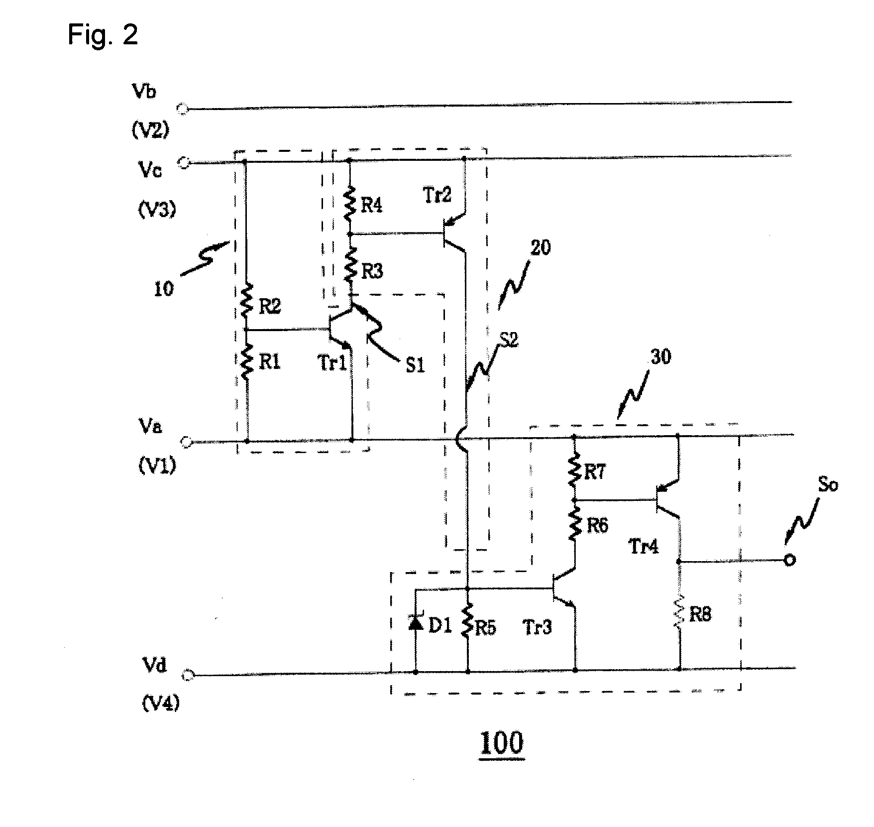
[0051]FIG. 2 is diagram showing the arrangement of a second preferred embodiment of the semiconductor device 100 of the present invention. The same numbers are used for the constituent elements that are the same as those shown in FIG. 1, and a detailed description thereof is omitted.

[0052] The detection circuit 10 includes a second resistor R2, one end of which is connected to the third terminal Vc, a first resistor R1 one end of which is connected to the first terminal Va, and the other end of which is connected to the other end of the second resistor R2, and an NPN-type first transistor Tr1 to the base terminal of which the connection point of the first resistor R1 and second resistor R2 is connected, and the emitter terminal of which is connected to the first terminal Va. The collector terminal of the first transistor Tr1 outputs the first output signal S1 as the output terminal of the detection circuit 10.

[0053] The operation of the detection circuit 10 will be described below...

third preferred embodiment

[0060]FIG. 3 is a diagram showing another preferred embodiment of the semiconductor device 100 of the present invention. The same numbers are used for constituent elements that are the same as those shown in FIG. 2, and a detailed description thereof is omitted. Because the only element that is different from FIG. 2 is the auxiliary circuit 20, a description of the detection circuit 10 and signal output circuit 30 is omitted.

[0061] The auxiliary circuit 20 includes a ninth resistor R9, one end of which is connected to the output of the detection circuit 10 (i.e., the collector terminal of the first transistor Tr1); an input-side transistor Tr5 of a current mirror the emitter terminal of which is connected to the third terminal Vc, and into which the first output signal S1 is input via the ninth resistor R9; and an output-side transistor Tr6 of the current mirror. Furthermore, the collector terminal of the output-side transistor Tr6 of the current mirror outputs the second output si...


PUM


Abstract

An electronic circuit includes a semiconductor device which has an internal circuit that uses a positive power supply voltage and a negative power supply voltage, and which controls the operation of the above-mentioned internal circuit by an external input. The semiconductor device includes an input signal detection circuit that operates using a voltage that is input into the external input, and a signal output circuit which outputs a signal that controls the negative power supply voltage applied to the internal circuit in accordance with an output of the input signal detection circuit. The circuit can switch a negative-side circuit on and off without depending on a positive power supply voltage and also without depending on the order of starting a positive power supply voltage and a negative power supply voltage.

Description

BACKGROUND OF THE INVENTION [0001] 1. Field of the Invention [0002] The present invention relates to a semiconductor device that has positive and negative power supply voltages and that does not depend on the order of the application of the power supplies. [0003] 2. Description of the Related Art [0004] In electrical devices using a plurality of voltages, there are cases in which the internal circuit must be controlled using a voltage that is lower than an ordinary reference voltage (e.g., 0 V). In the circuit shown in FIG. 7 in which the content of Japanese Patent Application Kokai No. S63-75810 is partially modified as one such example, the on / off control of a circuit 230 (hereinafter referred to as “negative-side circuit”) that uses a reference voltage GND and a voltage Vee (hereinafter referred to as “negative power supply voltage”) that is lower than this reference voltage as the operating voltage is performed by using a voltage Vcc (hereinafter referred to as “positive power s...

Claims


Application Information

Patent Timeline
IPC IPC(8): H03K5/22
CPCH03K5/08
Inventor KONDO, KENYA
Owner ROHM CO LTD
Why Eureka
Try Eureka