Chip and method for dicing wafer into chips

Active Publication Date: 2007-09-06
DENSO CORP
View PDF12 Cites 36 Cited by
  • Summary
  • Abstract
  • Description
  • Claims
  • Application Information

AI Technical Summary

Benefits of technology

[0046]According to a fourth aspect of the present disclosure, a chip includes: a first layer; a second layer disposed on the first layer. The first layer has a first periphery sidewall. The second layer has a second periphery sidewall. The second periphery sidewall includes a reforming region on t

Problems solved by technology

In this case, a process time for cutting the wafer is comparatively short.
However, the blade dicing method has the following difficulties.
Thus, a product yield of the chips is limited.
(2) When the wafer is cut by the dicing blade, abrasive heat and cutting scrap are generated.
However, in this case, a manufacturing cost may increase.
Further, even when the sealing with the seal member 17 is improved, it is difficult to prevent the water and the cutting scrap completely from penetrating into the construction 12.
Thus, the reflected laser beam

Method used


Image

  • Chip and method for dicing wafer into chips
  • Chip and method for dicing wafer into chips
  • Chip and method for dicing wafer into chips

Examples


first embodiment

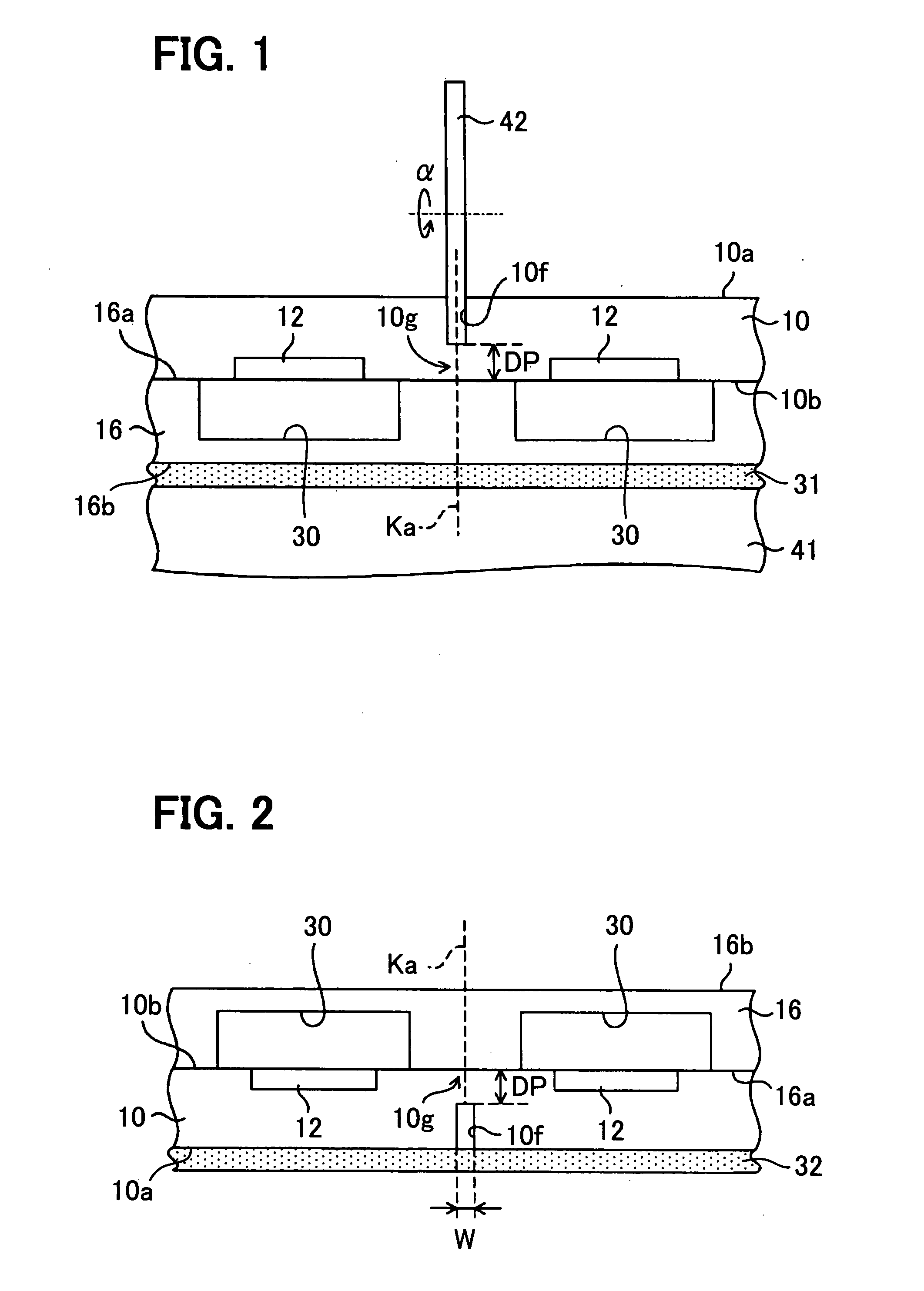
[0061]FIGS. 1 to 5 show a method for cutting a wafer 10 along with a cutting line Ka.

[0062]FIG. 1 shows a first step of the method for cutting the wafer 10. Firstly, a sealing film 31 is bonded to the surface 16b of the cap portion 16. Then, the backside 10a of the wafer 10 turns up, and the surface 16b of the cap portion 16 turns down. The wafer 10 is mounted on a stage 41, i.e., a specimen support of a blade dicing device so that the sealing film 31 contacts the top of the stage 41.

[0063]Then, a dicing blade 42 having a diamond abrasive grain embedded in the dicing blade 42 is rotated with high speed in a direction shown as a in FIG. 1. The rotating blade 42 press-contacts the backside 10a of the wafer 10 along with the cutting line Ka.

[0064]Thus, the wafer 10 is partially cut from the backside 10a so that a notch 10f is formed on the backside 10a of the wafer 10.

[0065]Then, the sealing film 31 is removed from the surface 16b of the cap portion 16. At this time, the wafer 10 is no...

second embodiment

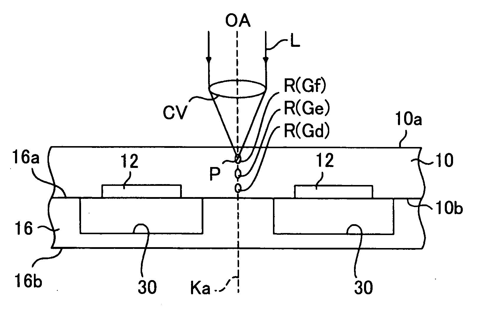
[0116]FIGS. 6 to 8 show a dividing step of the wafer 10 according to a second embodiment.

[0117]FIG. 6 shows a first step. The backside surface 10a of the wafer 10 turns up, and the wafer 10 is mounted on the laser beam processing device.

[0118]The laser beam processing device irradiates the laser beam L in a pulse manner on the backside surface 10a of the wafer 10 and focuses at the focus point P in the wafer 10. Further, the reforming regions R are formed in the wafer 10 along with the cutting line Ka by the multi photon absorption effect. The focus point P is displaced relative to the wafer 10, so that one reforming layer Gd-Gf composed of multiple reforming regions R is formed in the wafer 10. The reforming regions R in the one reforming layer Gd-Gf are arranged at predetermined intervals along with a predetermined horizontal direction parallel to the surface 10b and the backside surface 10a of the wafer 10.

[0119]The depth of the focus point P in the wafer 10 is changed in a stepw...

third embodiment

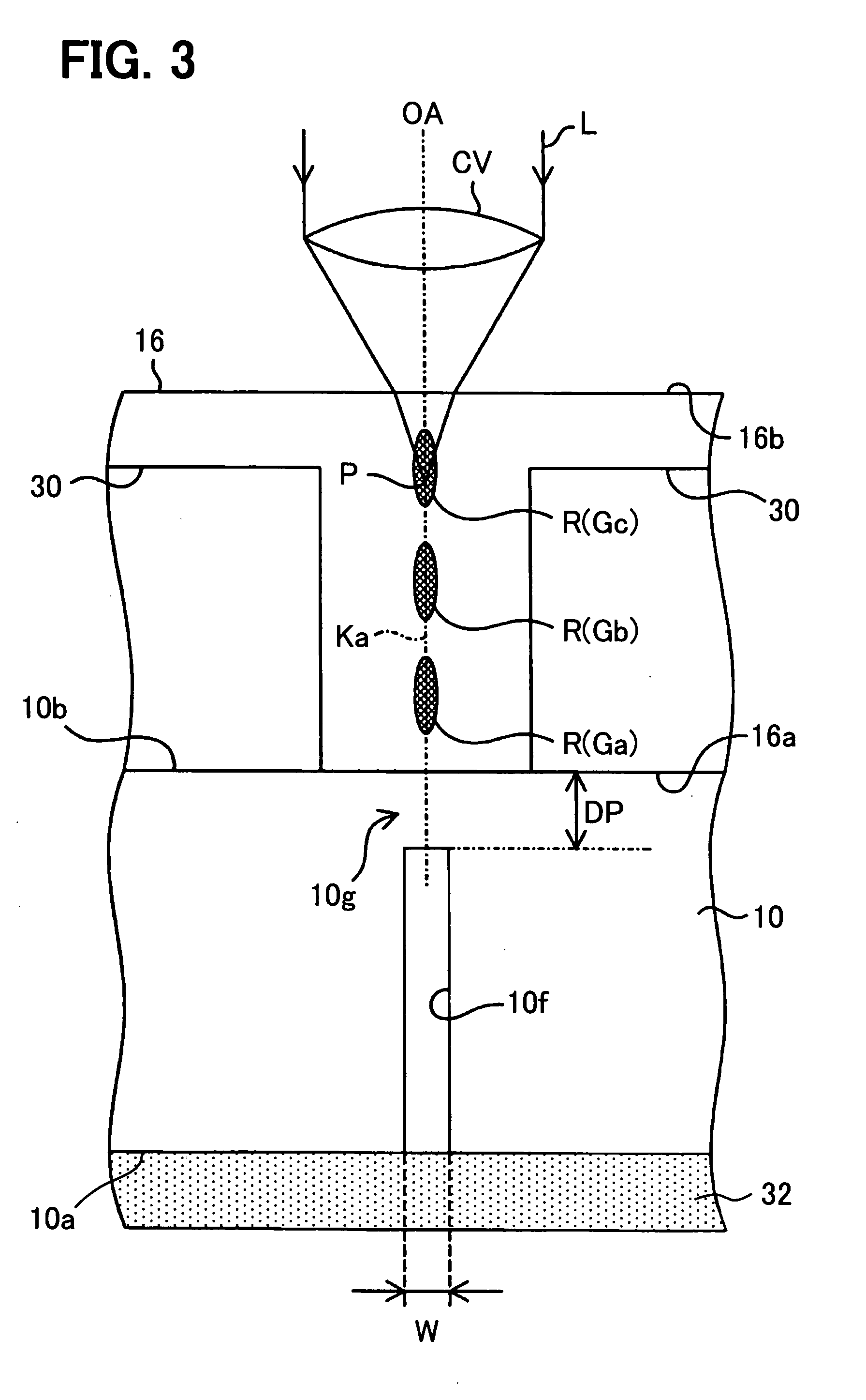
[0134]FIGS. 9 and 10 show a dividing step of the wafer 10 according to a third embodiment.

[0135]FIG. 9 shows a first step. The dicing film 32 is bonded to the surface 16b of the cap portion 16.

[0136]Then, the wafer 10 is mounted on the stage of the laser beam processing device under the condition that the backside 10a of the wafer 10 turns up.

[0137]The laser beam processing device forms the reforming layers Ga-Gc in the cap portion 16. Then, similar to the first step shown in FIG. 6, the reforming layers Gd-Gf are formed in the wafer 10.

[0138]FIG. 10 shows a second step. Similar to the fourth step shown in FIG. 5, the dicing film 32 is expanded in the horizontal direction γA-γB perpendicular to the cutting line Ka. Thus, the tensile stress is applied to the reforming layers Ga-Gf. Firstly, the cap portion 16 is cut and separated. Then, the wafer 10 is cut and separated. Accordingly, the chip 11 is separated from the wafer 10.

[0139]In FIG. 9, after the reforming layers Ga-Gc are form...


PUM

PropertyMeasurementUnit
Thicknessaaaaaaaaaa
Semiconductor propertiesaaaaaaaaaa

Abstract

A method for dicing a wafer including first and second layers is provided. A front surface of the first layer contacts a backside surface of the second layer. The method includes: forming a sealing film on the second layer; cutting the first layer from a backside surface along with a cutting line to form a notch; removing the sealing film; irradiating a laser beam on the front surface of the second layer along with the cutting line to form a reforming region in the second layer by a multi photon absorption effect; and dividing the wafer along with the cutting line from the reforming region as a starting point of dividing.

Description

CROSS REFERENCE TO RELATED APPLICATION[0001]This application is based on Japanese Patent Application No. 2006-57336 filed on Mar. 3, 2006, the disclosure of which is incorporated herein by reference.FIELD OF THE INVENTION[0002]The present invention relates to a chip and a method for dicing a wafer into chips.BACKGROUND OF THE INVENTION[0003]A laser dicing method for cutting an object such as a wafer into multiple chips by using a laser beam has been developed. For example, a focus of the laser beam is adjusted at an inside of the object, and the laser beam is irradiated on the object so that a reforming region is formed in the object. The reforming region is formed by a multi-photon absorption effect, and includes, for example, a crack, a melting region, or a region having a refraction index different from the object. The reforming region provides a starting point of cutting. The reforming region is formed along with a cutting line of the object such that the reforming region is dis...

Claims


Application Information

Patent Timeline
IPC IPC(8): H01L21/301B23K26/00B23K26/364B23K26/38
CPCB23K26/0057B23K26/4075H01L21/78H01L21/67132H01L21/67092B23K26/40B23K26/53B23K2103/50Y10T225/12
Inventor TAMURA, MUNEO
Owner DENSO CORP
Why Eureka
Try Eureka