Image display medium

a technology of image display and film, applied in the direction of electrical equipment, semiconductor devices, instruments, etc., can solve the problems of increasing the adhesive force and causing the peeling to occur, so as to prevent the warpage of plastic film, reduce the hygroscopicity of the coat layer, and prevent the wire break

Active Publication Date: 2007-09-13
E INK CORPORATION
View PDF2 Cites 1 Cited by
  • Summary
  • Abstract
  • Description
  • Claims
  • Application Information

AI Technical Summary

Benefits of technology

[0012]a coat layer is formed inside the at least one of the first substrate and the second substrate, and covering at least one of the first electrode and the second electrodes. Accordingly, the first and second electrodes can be protected and a wire break can be prevented. To use a composite polymer with inorganic particles dispersed as the coat layer, the residual stress of the coat layer is suppressed, whereby warpage of plastic film can be prevented and the hygroscopicity of the coat layer is decreased, whereby occurrence of crack of the transparent electrode caused by wrinkles occurring on the coat layer, etc., can be prevented.
[0013]The insulating layer has a thickness of 300 nm or more, and 30 μm or less. If the insulating layer has a thickness of 300 nm or more, it is preferable for ensuring an insulating property. If the layer is thick, the image force lowers and thus it is also preferable for preventing a burn error of display media. If the insulating layer has a thickness of 30 μm or less, it is preferable for circumventing the following problem: Because of excessive thickness, the electrode-to-electrode distance becomes long, the space volume required for obtaining a given electric field strength decreases, and flocculation of particles easily occurs.
[0014]Preferably, the insulating layer has predetermined hardness to prevent a display failure caused by an increase in the adhesive force with drive particles. If the hardness is too low, it is feared that the contact area with particles may increase because of deformation, causing the adhesive force to increase more than necessary.

Problems solved by technology

According to the image display medium, however, to sufficiently suppress the damage to the substrate caused by collision of the particles and the leakage of charges charged to the particles, the dielectric film needs to have a measure of thickness and as the thickness of the dielectric film increases, when bending deformation of the image display medium is performed, etc., it becomes impossible to follow the deformation, causing peeling to occur; this is a problem.
If the hardness is too low, it is feared that the contact area with particles may increase because of deformation, causing the adhesive force to increase more than necessary.

Method used


Image

  • Image display medium
  • Image display medium
  • Image display medium

Examples


first embodiment

(Advantages of First Embodiment)

[0044]According to the first embodiment, the following advantages are provided:

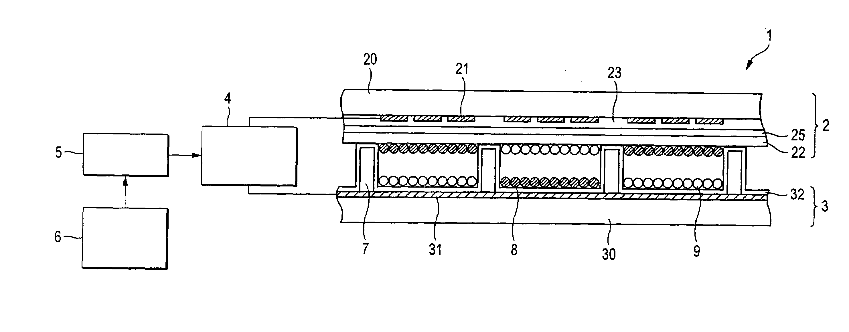
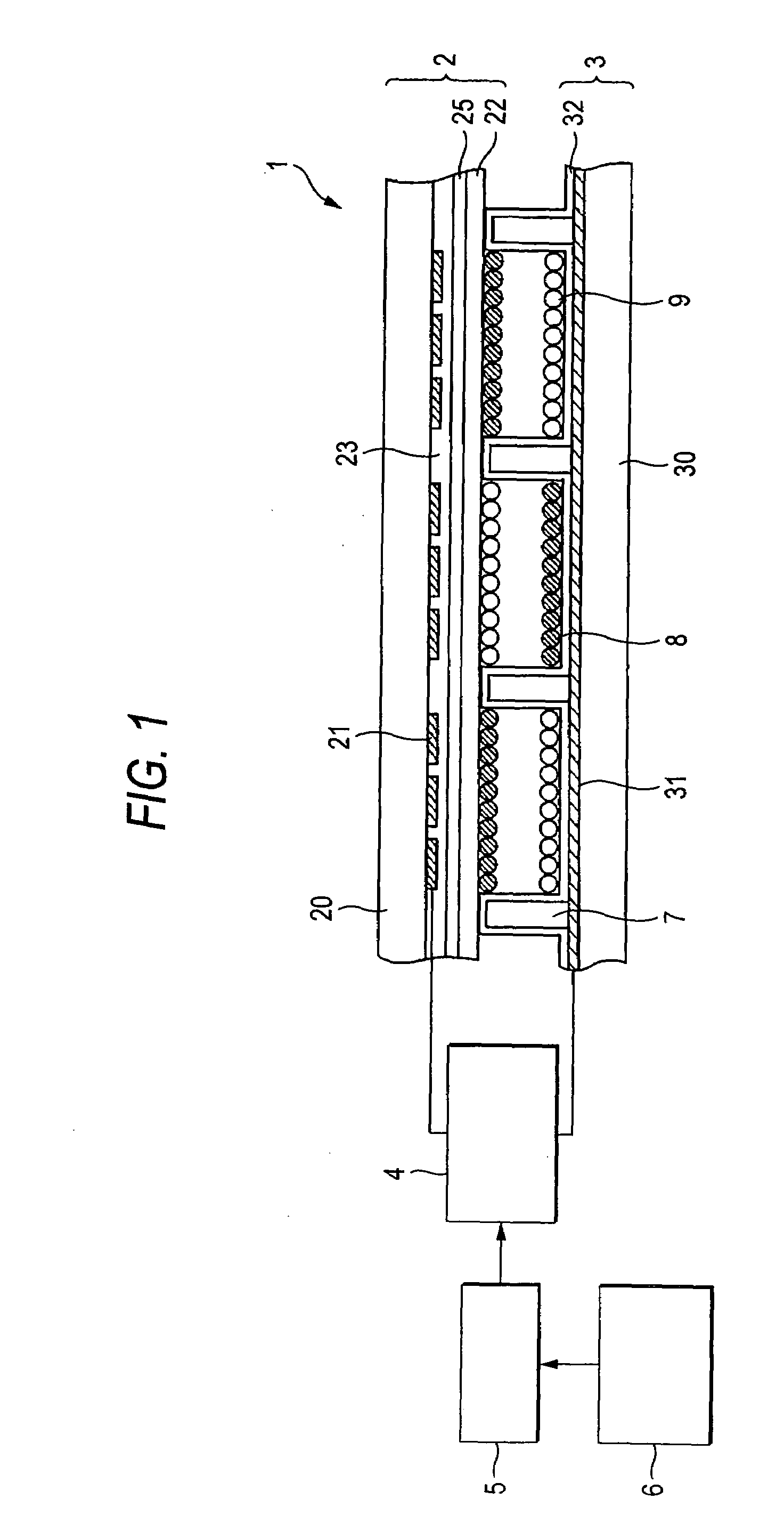
[0045](a) As the insulating layer 22 is formed through the first bonding layer 25 having a Young's modulus smaller than the surface support substrate 20 and the insulating layer 22, if the insulating layer 22 has a thickness to secure a sufficient insulating property, when bending deformation, etc., is added, the first bonding layer works as a buffer material and it is made possible for the insulating layer 22 to flexibly follow the deformation of the surface support substrate 20, so that peeling does not occur.

[0046](b) The insulating layer 22 is thickened, whereby occurrence of pinholes of the insulating layer 22 caused by collision of the first and second particles 8 and 9 can be suppressed and a display failure of the image display medium 1 caused by lowering of the charge amounts of the first and second particles 8 and 9 can be prevented.

Second Embodiment

[0047]FIG. 2 i...

second embodiment

(Advantages of Second Embodiment)

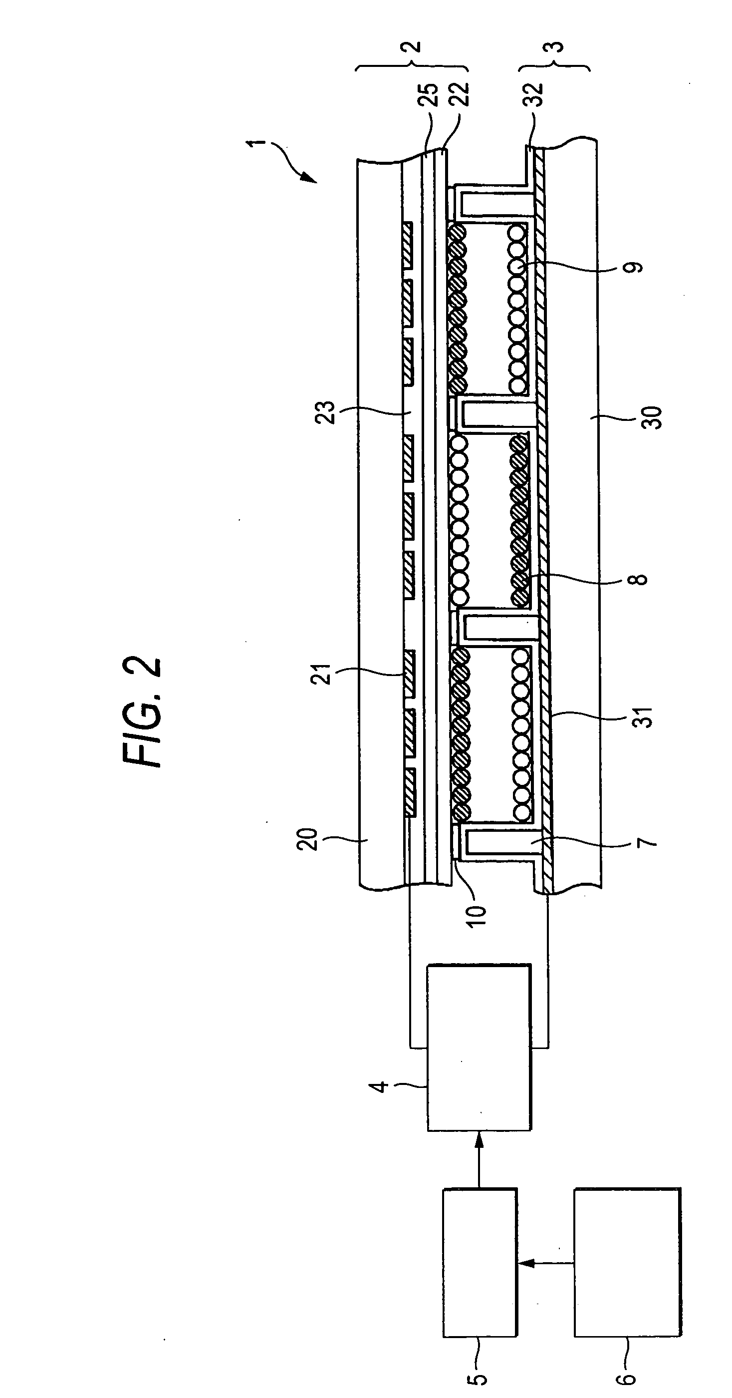
[0048]According to the second embodiment, when the partition members 7 and the insulating layer 22 are bonded by the second bonding layer 10, peeling occurring between the partition members 7 and the insulating layer 22 can be prevented.

Other Embodiments

[0049]It is to be understood that the invention is not limited to the specific embodiments thereof described above and various modifications and changes can be made without departing from the spirit and the scope of the invention.

[0050]For example, in the description of the embodiments, the first and second particles 8 and 9 are charged by friction, but the invention is not limited to the mode.

[0051]In the description of the embodiments, the image display medium 1 is a toner display, but may be any other type of image display medium for displaying an image with particles.

[0052]In the description of the embodiments, the image display medium 1 produces monochrome binary display, but may be an image disp...

first example

[0057]In a first example, four types of image display media 1 each having a similar configuration to that in the first embodiment were manufactured by changing the thickness of the insulating layer 22, and the charge amount of the mixed particles of white and black particles and the display density of each image display medium 1 were evaluated.

[0058]The thicknesses of the insulating layers 22 of the four types of image display media 1 were 0 (no insulating layer), 77 nm, 380 nm, and 1900 nm. Other components were common to the four types of image display media 1. The height of the partition member 7 was 200 μm, the thicknesses of the insulating film 32 was 1000 nm, and the diameter of a white particle charged negatively and the diameter of a black particle charged positively were each about 10 μm.

[0059]Transparent and colorless UV curable resin with tensile bonding force 80 kg / cm2 and Young's modulus 100 kg / cm2 was used as the first bonding layer 25. For the UV curable resin, curing...


PUM

PropertyMeasurementUnit
light transmittanceaaaaaaaaaa
thicknessaaaaaaaaaa
thicknessaaaaaaaaaa

Abstract

An image display medium includes: a first substrate; a second substrate facing the first substrate; a first bonding layer provided inside at least one of the first substrate and the second substrate; and an insulating layer fixed to the at least one of the first substrate and the second substrate by the first bonding layer, wherein the first bonding layer has a Young's modulus smaller than the substrate formed with the insulating layer and the insulating layer.

Description

BACKGROUND[0001]1. Technical Field[0002]This invention relates to an image display medium having flexibility and in particular to an image display medium having an insulating film inside a substrate.[0003]2. Related Art[0004]Hitherto, an image display medium for displaying an image using charged toner particles of two colors has been available as an image display medium having flexibility such as electronic paper.[0005]The image display medium includes a pair of substrates placed facing each other, a spacer sandwiched between the pair of substrates, and first and second particles different in color and electronic characteristic, filled into internal space between the substrate and the spacer.[0006]According to the image display medium, a dielectric film is provided inside the substrate, whereby damage to the substrate caused by collision of the particles and leakage of charges charged to the particles are suppressed for preventing degradation of the image display characteristic.[000...

Claims


Application Information

Patent Timeline
Patent Type & Authority Applications(United States)
IPC IPC(8): H01L29/04G02F1/167G02F1/16756
CPCG02F2202/28G02F1/167G02F1/16756
Inventor HIRANO, ATSUSHISUWABE, YASUFUMIMACHIDA, YOSHINORIYAMAGUCHI, YOSHIROMATSUNAGA, TAKESHISHIGEHIRO, KIYOSHI
Owner E INK CORPORATION
Why Eureka
Try Eureka