Nitride semiconductor light emitting device
a light-emitting device and semiconductor technology, applied in semiconductor devices, semiconductor lasers, lasers, etc., can solve the problems of reducing reliability and degradation of the light-emitting portion, and achieve the effect of improving reliability and high power driv
- Summary
- Abstract
- Description
- Claims
- Application Information
AI Technical Summary
Benefits of technology
Problems solved by technology
Method used
Image

Examples
first embodiment
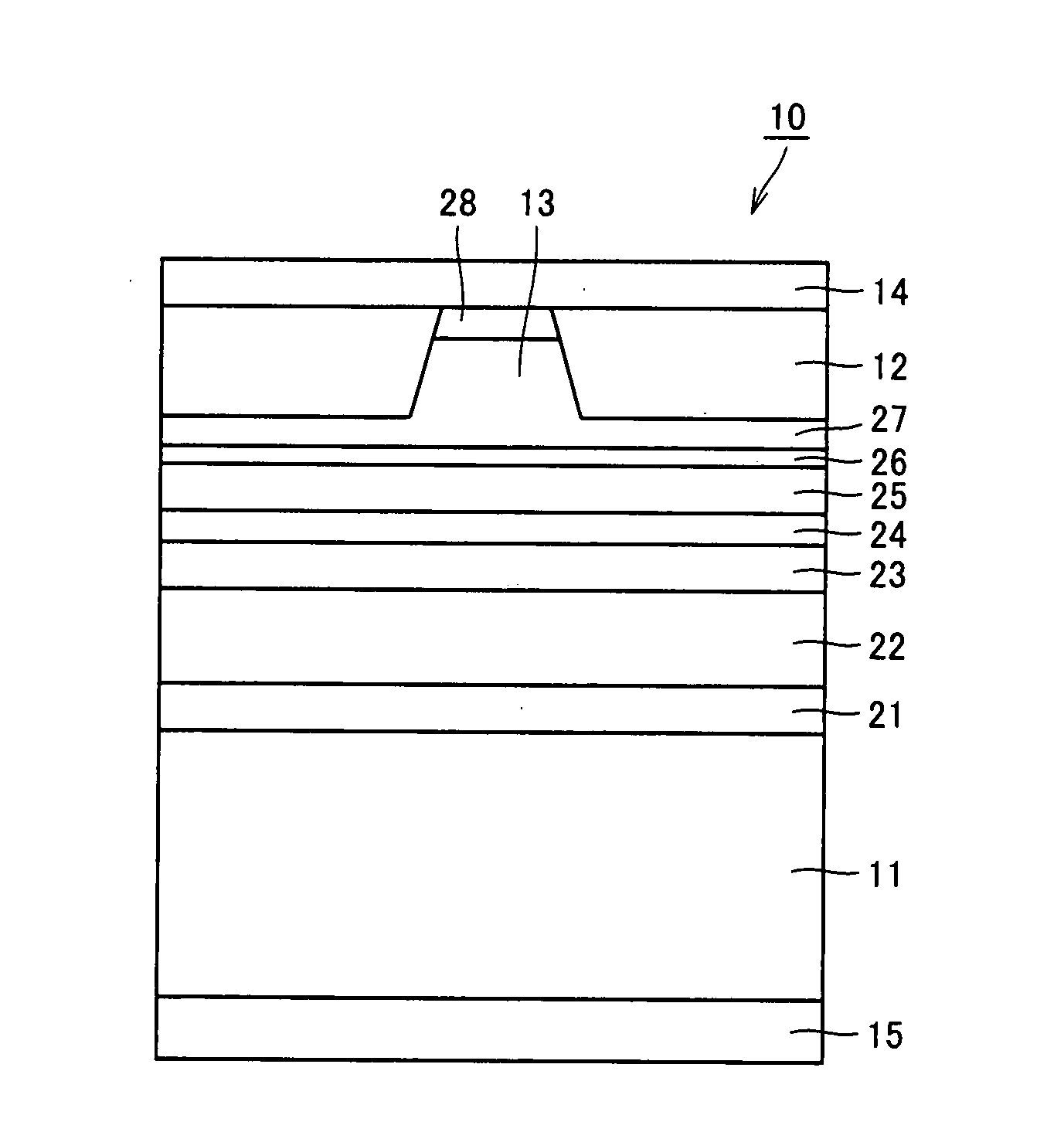
[0047]FIG. 1 is a cross section schematically showing a nitride semiconductor laser device in the present embodiment. Here, a nitride semiconductor laser device 10 in the present embodiment is configured to include a buffer layer 21 having a thickness of 0.2 μm made of n-type GaN, an n-type cladding layer 22 having a thickness of 2.3 μm made of n-type Al0.06Ga0.94N, an n-type guide layer 23 having a thickness of 0.02 μm made of n-type GaN, a multiple quantum well active layer 24 made of 4 nm-thick InGaN and 8 nm-thick GaN, a protective layer 25 having a thickness of 70 nm made of GaN, a p-type current block layer 26 having a thickness of 20 nm made of p-type Al0.3Ga0.7N, a p-type cladding layer 27 having a thickness of 0.5 μm made of p-type Al0.05Ga0.95N, and a p-type contact layer 28 having a thickness of 0.1 μm made of p-type GaN, which are stacked on a semiconductor substrate 11 made of n-type GaN in this order from semiconductor substrate 11. Here, the thickness and mixed crysta...
second embodiment
[0081]A nitride semiconductor laser device in the present embodiment has the similar configuration as the nitride semiconductor laser device in the first embodiment, except that the respective configurations of films formed on the facets at the light emitting side and the light reflecting side are changed and that the wavelength of emitted laser light is set at 410 nm.
[0082]Here, in the nitride semiconductor laser device in the present embodiment, respective aluminum nitride films each having a thickness of 6 nm are formed on the facets at the light emitting side and at the light reflecting side, and an aluminum oxide film having a thickness of 80 nm is formed on each of the aluminum nitride films. Here, the reflectivity at the light emitting side is set to 7%. The aluminum nitride film and the aluminum oxide film are formed by ECR sputtering. Specifically, deposition was performed without introducing oxygen gas, which is introduced in the first embodiment to form an aluminum oxynit...
third embodiment
[0084]A nitride semiconductor laser device in the present embodiment has the similar configuration as the nitride semiconductor laser device in the first embodiment, except that the respective configurations of films formed on the facets at the light emitting side and the light reflecting side are changed and that the wavelength of emitted laser light is set at 400 nm.
[0085]Here, in the nitride semiconductor laser device in the present embodiment, respective aluminum oxynitride films each having a thickness of 12 nm are formed on the facets at the light emitting side and at the light reflecting side, and an aluminum oxide film having a thickness of 80 nm is formed on each of the aluminum oxynitride films. Here, the reflectivity at the light emitting side is set to 10%. On the facet at the light reflecting side, a high reflection film having an identical configuration to that of the first embodiment is formed on the aluminum oxide film.
[0086]For the nitride semiconductor laser device...
PUM
 Abstract
Description
Claims
Application Information
 - R&D
- Intellectual Property
- Life Sciences
- Materials
- Tech Scout
- Unparalleled Data Quality
- Higher Quality Content
- 60% Fewer Hallucinations
Browse by: Latest US Patents, China's latest patents, Technical Efficacy Thesaurus, Application Domain, Technology Topic, Popular Technical Reports.
© 2025 PatSnap. All rights reserved.Legal|Privacy policy|Modern Slavery Act Transparency Statement|Sitemap|About US| Contact US: help@patsnap.com