Switching transistor driver circuit

Inactive Publication Date: 2007-09-13
PANASONIC SEMICON SOLUTIONS CO LTD
View PDF7 Cites 27 Cited by
  • Summary
  • Abstract
  • Description
  • Claims
  • Application Information

AI Technical Summary

Benefits of technology

[0049]Particularly in the case where the load connected to the output terminal includes a coil, in a dead time period during which the low-side switching transistor and the high-side switching transistor are both turned off immediately after the high-side switching transistor switches from on to off in a state in which the low-side switching transistor is turned off, the terminal voltage of the output terminal for driving the load has a negative potential reduced fro

Problems solved by technology

However, the conventional switching transist

Method used


Image

  • Switching transistor driver circuit
  • Switching transistor driver circuit
  • Switching transistor driver circuit

Examples


embodiment 1

[0073]The following will describe a switching transistor driver circuit according to Embodiment 1 of the present invention.

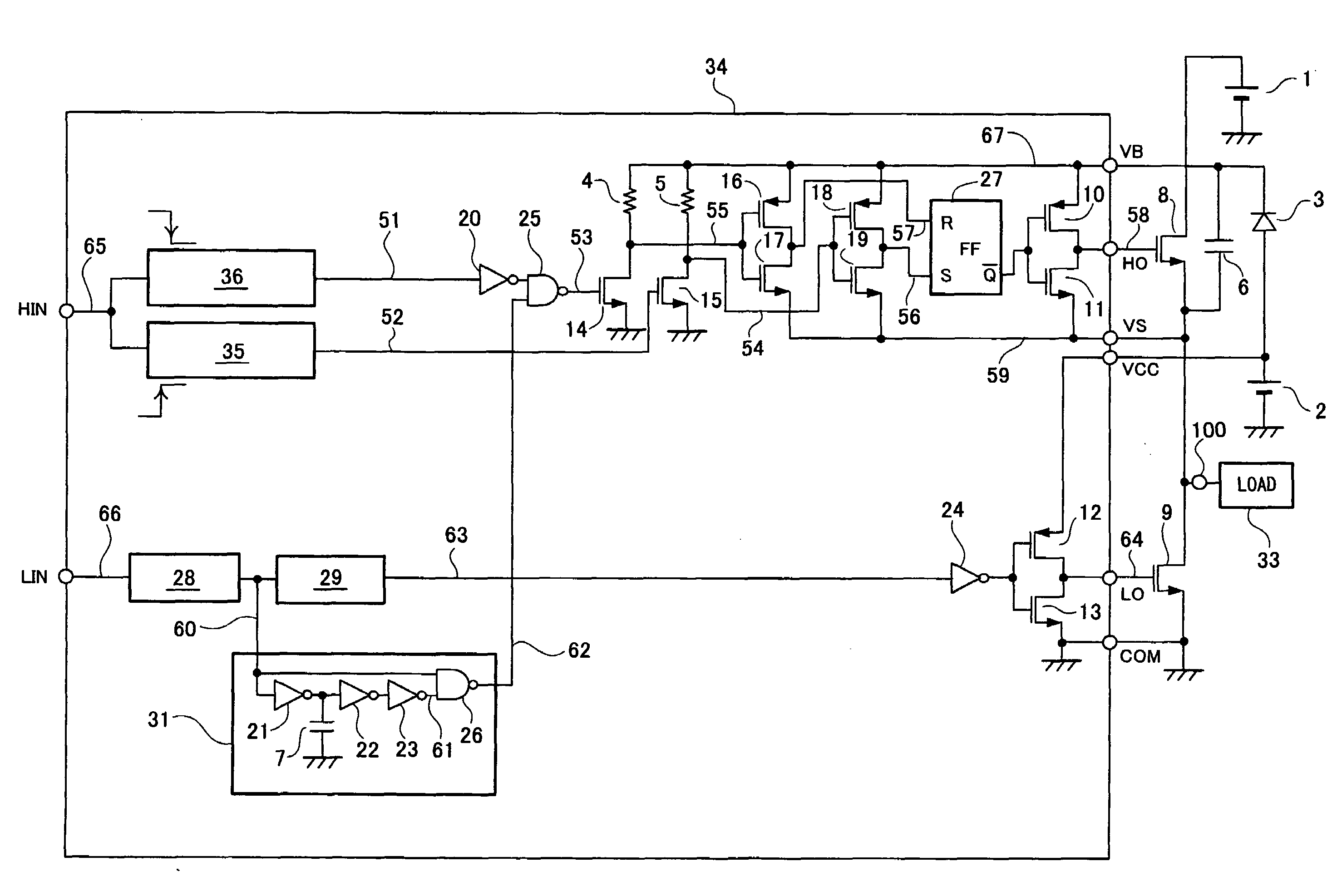
[0074]FIG. 1 shows the switching transistor driver circuit of the present invention. Reference numeral 1 denotes a high voltage power supply, reference numeral 2 denotes a low voltage power supply, reference numeral 3 denotes a diode, reference numerals 4 and 5 denote resistors, reference numeral 6 and 7 denote capacitors, and reference numerals 8 and 9 denote power N-channel MOS transistors (hereinafter, will be referred to as transistors) serving as a pair of switching transistors connected in series. In this configuration, the transistor 8 on the high potential side is a high-side switching transistor and the transistor 9 on the low potential side is a low-side switching transistor. Reference numerals 10 and 12 denote output P-channel MOS transistors (hereinafter, will be referred to as transistors), reference numerals 11 and 13 denote output N-channel MOS tr...

embodiment 2

[0099]The following will describe a switching transistor driver circuit according to Embodiment 2 of the present invention.

[0100]FIG. 6 shows the switching transistor driver circuit of the present invention. Reference numeral 68 denotes a delay circuit obtained by combining the delay circuit 28 and the delay circuit 29 of FIG. 1, reference numeral 69 denotes a delay circuit having a low side input terminal LIN as an input and an output connected to the input of a reset pulse generation circuit 31, reference numerals 70 and 71 denote signal lines, and reference numeral 72 denotes a circuit included in a semiconductor integrated circuit. Other components are similar to those of FIG. 1.

[0101]In FIG. 1, a delay time from the low side input terminal LIN to the reset pulse generation circuit 31 is set by the delay circuit 28. FIG. 6 is different only in that the delay circuit 69 is additionally provided between the low side input terminal LIN and the reset pulse generation circuit 31. The...

embodiment 3

[0103]A switching transistor driver circuit according to Embodiment 3 of the present invention will now be described below.

[0104]FIG. 7 shows the switching transistor driver circuit of the present invention. Reference numeral 68 denotes a delay circuit obtained by combining the delay circuit 28 and the delay circuit 29 of FIG. 1, reference numeral 93 denotes a P-channel MOS transistor (hereinafter, will be referred to as a transistor), reference numeral 94 denotes an N-channel MOS transistor (hereinafter, will be referred to as a transistor), reference numeral 95 denotes a resistor, reference numeral 96 denotes a capacitor, reference numeral 97 denotes an inverter, reference numeral 99 denotes a delay circuit, reference numerals 74, 75, 76 and 77 denote signal lines, and reference numeral 78 denotes a circuit included in a semiconductor integrated circuit. Other components are similar to those of FIG. 1.

[0105]FIG. 8 is a timing chart for explaining the circuit operations of FIG. 7. ...


PUM


Abstract

Of a pair of switching transistors connected in series between a high voltage power source and the ground, when the switching transistor on the high potential side is controlled by an RS flip-flop in response to an input signal, in order to prevent a malfunction caused by the influence of dv/dt transient phenomena of an output terminal for driving a load, a latch circuit is reset using an input signal from a low side input terminal LIN in a period during which the voltage of the output terminal for driving the load abruptly decreases.

Description

FIELD OF THE INVENTION[0001]The present invention relates to a switching transistor driver circuit for controlling a pair of switching transistors connected in series such that power supply to a load is controlled based on a pulse signal fed to a high side input terminal and a low side input terminal.BACKGROUND OF THE INVENTION[0002]This kind of switching transistor driver circuit is disclosed in Japanese Patent Laid-Open No. 4-230117. The circuit is configured as shown in FIG. 15.[0003]In this configuration, when a load 230 is driven by a high voltage power supply 228, voltage is applied from the high voltage power supply 228 to a series circuit of a pair of power N-channel MOS transistors (hereinafter, will be referred to as transistors) 224 and 225, and the load 230 is connected to a junction point of the source of the transistor 224 and the drain of the transistor 225. Of the transistors 224 and 225, the transistor 224 on the high potential side is turned on / off by a pulse signa...

Claims


Application Information

Patent Timeline
IPC IPC(8): G05F1/00
CPCH03K17/162H03K17/6871H03K2217/0036H03K19/00361H03K19/018521H03K19/0013H03K2217/0063
Inventor KATAOKA, SHINICHIRO
Owner PANASONIC SEMICON SOLUTIONS CO LTD
Why Eureka
Try Eureka